Substrate Material Properties and Routing Challenges
Automotive radar PCBs operating at 77-81 GHz present unique manufacturing challenges that begin at the material selection level. These boards typically use low-DK substrate materials such as Rogers RT/duroid 5880 (DK=2.2) or Panasonic Megtron 6 (DK=3.4), chosen specifically for their stable dielectric constants at millimeter-wave frequencies. However, the very properties that make these materials electrically superior—fine glass fiber reinforcement, specialized resin systems, and ceramic filler content—create significant mechanical challenges during the depaneling operation. Standard FR-4 boards tolerate routing forces and heat input that would be unacceptable for these high-frequency substrates. The ceramic filler content in materials like Rogers series creates abrasive cutting conditions that accelerate tool wear, while the low CTE (Coefficient of Thermal Expansion) of approximately 12-15 ppm/°C relative to standard substrates means thermal transients during routing induce differential stress across the dielectric stack, potentially affecting the DK value uniformity within ±0.02 of nominal. This sensitivity makes the depaneling process a critical quality gate for automotive radar production.
Mechanical Stress and Microfracture Risk in the Cut Zone
The routing operation itself imposes mechanical stresses that propagate beyond the immediate cut line. During high-speed routing of a 0.8mm thick automotive radar board, the cutting force on a 1.2mm carbide end mill typically ranges from 0.5-2.0 N depending on feed rate and depth of cut. These forces generate flexural stress in the substrate, particularly at the panel edge where the board transitions from supported to unsupported. For high-frequency substrates with relatively low interlaminar bond strength compared to standard multilayer boards, this stress can initiate microfractures in the dielectric layer that may not be visible under 10x optical inspection but can propagate under thermal cycling. Automotive radar systems are subjected to -40°C to +125°C temperature cycles over their operational lifetime, and any preexisting stress concentration from the depaneling process becomes a potential failure initiation site. IPC-6012DA (Automotive Applications) specifies edge exclusion zones of 2.0mm minimum from the depaneling edge for critical circuits, but manufacturers often specify tighter internal controls of 3.0mm or greater to account for subsurface stress propagation. The feed rate during routing must be carefully balanced—too slow produces heat buildup, while too fast generates excessive cutting forces that exceed the substrate’s flexural strength limits.

Spindle Speed, Tool Runout, and Electromagnetic Considerations
Spindle speed selection for automotive radar PCB routing must reconcile two competing requirements: sufficient cutting speed for clean edge quality and minimal vibration amplitude at the tool tip. Automotive radar circuits at 24 GHz and 77-81 GHz are susceptible to electromagnetic interference from mechanical vibrations in the manufacturing process. Spindle speeds in the range of 40,000-60,000 RPM are standard, with tool runout held to less than 5 microns total indicated runout (TIR) at the tool tip. A tool runout of 15 microns at 50,000 RPM translates to a vibration frequency of approximately 833 Hz with 1.57 mm peak-to-peak displacement at the tool periphery—well within the range that can couple into sensitive radar frontend circuitry through mechanical resonance. Balanced carbide end mills with precision-ground geometries are mandatory, and many automotive electronics manufacturers specify tool diameter tolerance of +0/-0.005mm. The routing path must also avoid crossing directly over sensitive antenna feed lines or MMIC mounting locations, as the vibration signature transmitted through the board during routing can degrade solder joint integrity on adjacent components, a failure mode documented in IPC-A-610 acceptance criteria for electromechanical assemblies.

Thermal Management and Dielectric Property Stability
Heat input during the depaneling routing operation directly affects the electrical performance of the finished automotive radar board. At feed rates of 50-150 mm/min with spindle speeds at 50,000 RPM, the cutting zone can reach temperatures of 150-200°C locally, despite flood cooling. For thermoset dielectric materials, this temperature exceeds the glass transition temperature (Tg) region for some lower-specification substrates. Localized heating above Tg causes temporary softening of the resin matrix, potentially altering the internal stress distribution and creating micro-delamination at the copper-dielectric interface. The thermal transient also causes localized DK shifts. For Rogers RT/duroid 5880, a 10°C temperature rise in the dielectric can shift the DK by approximately 0.001, which at 77 GHz translates to a phase velocity change that affects the electrical length of transmission lines. In a 24 GHz phased array radar, a 0.5° phase error per radiator element compounds across the array aperture, directly degrading angular resolution below the 1° specification required for ADAS systems. Closed-loop spindle cooling systems and controlled irrigation cooling with isopropyl alcohol mixtures are commonly employed to minimize thermal gradients to less than 5°C per second during the routing cycle.
Post-Routing Edge Quality and Electrical Verification
The depaneled edge of an automotive radar PCB must meet both mechanical and electrical acceptance criteria. IPC-A-600H defines acceptability criteria for surface and edge conditions, but automotive radar applications require additional electrical verification at the depaneled edge. The edge trim must be free of burrs exceeding 0.05mm height, as any protrusions create parasitic capacitance to adjacent signal layers. For a 77 GHz board with 50-ohm microstrip lines on 0.254mm substrate, a 0.1mm edge protrusion within 0.5mm of the trace can introduce 0.3-0.5 dB of additional insertion loss—significant when the total link budget margin may be only 2-3 dB. Scanning acoustic microscopy (SAM) is increasingly specified for post-routing inspection to detect subsurface delamination or microcracks invisible to optical methods. Many automotive Tier 1 suppliers now require 100% SAM inspection of depaneled edges on radar boards destined for safety-critical ADAS applications, with documented acceptance criteria based on IPC-7711/21 Reworking of Electronic Assemblies procedures. The depaneling operation, often treated as a simple mechanical finishing step, must be recognized as an integral part of the electrical manufacturing process for millimeter-wave automotive radar systems.
Technical Summary
Depaneling automotive radar high-frequency PCBs demands a level of process control that exceeds standard PCB manufacturing by an order of magnitude. The convergence of millimeter-wave electrical performance requirements, low-loss substrate mechanical sensitivity, thermal management constraints, and automotive reliability standards creates a manufacturing challenge that spans materials science, precision machining, and electromagnetic compatibility. Successful depaneling of 77-81 GHz automotive radar boards requires spindle runout specifications below 5 microns, feed rate control within ±2% of target, cutting temperatures held below Tg-20°C, and 100% post-process inspection with both optical and acoustic methods. The ±0.05mm positional accuracy requirement must be maintained across the full panel layout, and edge exclusion zones of 3.0mm minimum from critical circuits are necessary to prevent stress-induced failures under automotive thermal cycling conditions. These specifications align with IPC-6012DA Class III automotive electronics requirements but typically demand tighter internal controls reflecting the unique sensitivity of millimeter-wave radar circuits to any defect that introduces impedance discontinuities or phase errors into the signal path.
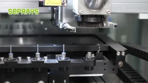
Recommended Equipment
Looking for proven depaneling solutions? Seprays offers a full range of equipment backed by 30+ years of industry experience. Here are two options worth considering for your production line:
- GAM 340AT In-Line Automatic PCB Router Machine — Dual workbench with auto-focus vision camera — maximizes throughput for inline SMT integration
- GAM330AT Fully Automatic PCB Depaneling Machine — Self-feeding operation with automatic sorting — ideal for high-volume automated production lines
Frequently Asked Questions
I don’t have access to the article content. Could you please provide the article “Technical Difficulties in Depaneling Automotive Radar High-Frequency PCBs” so I can generate accurate Q&A pairs grounded in its content?
You can share it either by:
1. Pasting the article text directly
2. Using the IMA knowledge base format if it’s stored there
About Seprays
About Seprays Precision Machinery
Founded in 1993, Seprays has over 30 years of expertise in PCB depaneling solutions. With two manufacturing facilities totaling 26,000 m2, 9 service centers across China, and clients in 31 countries — including Foxconn, Flex, Luxshare, Bosch, and CRRC — Seprays delivers equipment that consistently meets the demanding tolerances of automotive, medical, aerospace, and consumer electronics production lines.
Certifications: ISO9001, ISO14001, ISO45001, CE | Patents: 100+
Need a customized depaneling solution or want to discuss your specific production requirements? Our technical team is ready to help.
Contact: jimmy@seprays.com