Flexible PCB depaneling for smart wearables demands positional accuracy within ±0.02mm, as the typical copper trace width on wearable FPCBs ranges from 0.075mm to 0.1mm—leaving virtually no margin for routing deviation. A single misplaced cut can sever signal traces, short adjacent circuits, or induce micro-cracks in the polyimide substrate that propagate under flex cycling. Unlike rigid PCBs where tolerances of ±0.05mm are often acceptable, flexible circuits in smartwatches, fitness bands, and medical wearables operate in a dynamic mechanical environment where cut-edge quality directly impacts product longevity. Industry data indicates that edge delamination failures in wearables correlate strongly with depaneling method: punched boards show 3.2x higher failure rates in flex testing compared to laser-cut or precision-routed alternatives.
Mechanical Stress and Cutting Mechanics
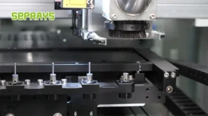
The fundamental challenge in FPCB depaneling lies in minimizing mechanical stress transmitted to the substrate. Traditional V-scoring, which exerts 15-25 N/mm of blade force, is unsuitable for flexible materials—the polyimide base (typical thickness 25-125μm) cannot absorb this compressive load without substrate damage. Router-based depaneling systems designed for flexible circuits typically employ high-speed spindles operating at 40,000-80,000 RPM with feed rates reduced to 5-15 mm/sec, compared to 30-50 mm/sec for rigid boards. The cutting force must remain below 2-3 N to prevent workpiece distortion, requiring precision spindle runout specifications below 5μm TIR (Total Indicated Runout). Research on delamination initiation shows that cutting forces exceeding 4N create interlaminar stresses in the adhesive layer that exceed the peel strength of typical flexible laminate systems (typically 1.0-1.5 N/mm).
Laser Depaneling Technology
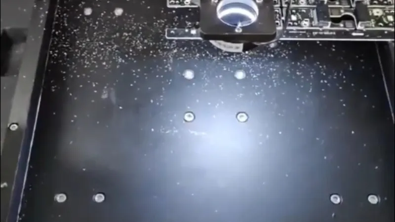
UV laser systems (355nm wavelength) have become the dominant technology for flexible PCB depaneling in high-volume wearable manufacturing, offering kerf widths of 20-50μm with heat-affected zones (HAZ) controlled to under 30μm when properly tuned. Pulse duration is critical: nanosecond lasers (3-10ns pulse width) produce HAZ of 50-100μm, while picosecond lasers (10-15ps) reduce thermal damage to under 15μm—essential for circuits with 0.5mm trace spacing or less. Typical processing parameters for 100μm-thick FPCBs include laser power of 8-15W, pulse repetition rates of 100-500kHz, and cutting speeds of 100-300 mm/sec depending on material composition. IPC-6013 class 3 requirements specify that laser-cut edges shall be free of carbonization exceeding 25μm in depth, necessitating process optimization for each laminate stackup. Edge roughness (Ra) achievable with optimized laser parameters ranges from 1.5-3.0μm, compared to 5-15μm for mechanical routing.
Material Considerations for Wearable FPCBs
Flexible circuits in smart wearables typically use adhesive-based or adhesiveless laminate constructions. Adhesive-based systems (polyimide + acrylic or epoxy adhesive + copper) present higher risk during thermal cutting due to outgassing—measured mass loss rates of 0.8-1.2% at cutting temperatures can deposit residue on optical components and create porosity along cut edges. Adhesiveless laminates (cast polyimide directly on copper) show superior edge quality with laser processing, exhibiting carbonization depths 40-60% lower than adhesive-based equivalents. Bend radius specifications for wearable FPCBs typically require minimum static bend radii of 3-6x the circuit thickness, making edge integrity critical: a 20μm chip-out or crack initiation site can propagate to failure within 10,000-50,000 flex cycles in typical wrist-worn applications. Copper thickness variations (12μm, 17μm, 35μm standard) affect both mechanical routing loads and laser energy absorption, requiring parameter adjustments of 15-25% between stackups.

Fixture Design and Positional Accuracy
Smart wearable FPCBs often measure 20-60mm in maximum dimension with tab widths as narrow as 1.5-2.5mm for connecting to carrier panels. Conventional pin-based tooling cannot accommodate these geometries without inducing stress—fixture pressure exceeding 0.15 MPa at holding points can create localized substrate deformation visible under magnification. Vacuum table systems with porous ceramic or aluminum surfaces provide uniform workholding with pressure differentials of 60-85 kPa, sufficient to restrain thin flexible materials without mechanical damage. Positional repeatability requirements for depaneling systems targeting wearable FPCBs typically specify ±0.02mm over a 100mm working area, with vision systems capable of fiducial recognition accuracy within ±5μm. Multi-panel carrier designs common in wearable manufacturing (panel sizes 250×350mm or 300×400mm) require automatic panel alignment routines compensating for FPCB dimensional stability variations of 0.05-0.15% due to lamination shrinkage and moisture absorption effects.
Process Validation and Quality Metrics
IPC-6013 and IPC-A-600 provide acceptance criteria for flexible circuit depaneling, but wearable applications often require supplementary specifications. Edge quality inspection typically includes measurement of burr height (maximum 25μm for class 3, though wearable specifications often reduce this to 10-15μm), chip-out depth, and delamination extent. Cross-sectional analysis of routed edges should show continuous copper and dielectric layers without interlaminar separation. Statistical process control for depaneling operations tracks first-pass yield (target 99.5%+ for mature processes), with common failure modes including dimensional deviation (55% of failures), edge quality defects (25%), and substrate damage (20%). In-line inspection systems using high-resolution cameras (5μm pixel resolution minimum) combined with edge-detection algorithms can achieve 99% detection rates for defects exceeding 50μm, though sub-25μm defects typically require sampling-based microscopic inspection. Correlation studies between depaneling parameters and field failure rates show that each 10μm increase in average edge roughness correlates with a 0.3% increase in flex-fatigue failures at 25,000 cycles.
Technical summary: Effective flexible PCB depaneling for smart wearables requires matching depaneling technology to material construction and end-use mechanical demands. UV laser systems achieve the tightest tolerances (±0.02mm positional, <30μm HAZ) with highest throughput for thin flexible circuits, while precision routing remains viable for thicker constructions or metallic stiffener regions. Critical parameters include spindle runout below 5μm for mechanical cutting, pulse duration under 15ps for laser processing of fine-pitch circuits, and fixture designs that limit substrate stress to under 0.15 MPa. Process validation must extend beyond IPC requirements to include application-specific flex testing correlating edge quality to predicted device lifespan in dynamic wearable environments.
Recommended Equipment
Looking for proven depaneling solutions? Seprays offers a full range of equipment backed by 30+ years of industry experience. Here are two options worth considering for your production line:
- ZM30-D Multi-Tool Multi-Group PCB Depaneling Machine — One-time full LED board cutting — daily output exceeding 100,000 pieces with custom configurations
- GAM300AT Double-Layer Track Online PCB Board Separation Machine — Full-carrier process with carrier return track — built for seamless full-line automation
Frequently Asked Questions
I don’t see the article content in your message. Could you please provide the article about “Industry Solutions for Flexible PCB Depaneling in Smart Wearables” so I can generate accurate Q&A pairs grounded in its content?
You can either:
1. Paste the article text directly
2. Provide a file path if it’s saved locally
3. Share a URL to the article
Once I have the article content, I’ll generate exactly 3 practical Q&A pairs in the HTML format you specified.
About Seprays
About Seprays Precision Machinery
Founded in 1993, Seprays has over 30 years of expertise in PCB depaneling solutions. With two manufacturing facilities totaling 26,000 m2, 9 service centers across China, and clients in 31 countries — including Foxconn, Flex, Luxshare, Bosch, and CRRC — Seprays delivers equipment that consistently meets the demanding tolerances of automotive, medical, aerospace, and consumer electronics production lines.
Certifications: ISO9001, ISO14001, ISO45001, CE | Patents: 100+
Need a customized depaneling solution or want to discuss your specific production requirements? Our technical team is ready to help.
Contact: jimmy@seprays.com