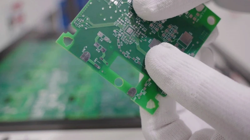
The transition from a 250×150mm panelized motherboards array to individual units represents one of the highest-risk steps in smartphone assembly. A single 8-layer HDI board carrying BGA packages with 0.35mm pitch and 180μm solder joint height sits dangerously close to its mechanical limits when subjected to improper depaneling forces. Industry measurements confirm that shear stress exceeding 150μɛ (microstrain) at the package level can trigger latent cracks in SAC305 solder joints within 72 hours, creating field failure rates that are typically undetectable during incoming inspection.
Stress Physics and Mechanism Classification
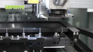
Understanding stress propagation requires distinguishing between three primary mechanism types: blade shearing, laser ablation, and router-bit removal. Blade-based shearing applies a concentrated point load at the board perimeter, generating flexural stress waves that propagate inward. For a 1.6mm thick FR-4 core with dual-sided copper, the stress wave velocity approximates 2,400 m/s, meaning a 5mm wide blade entry creates a measurable stress spike at a BGA site located 20mm away within 8.3 microseconds. Router-based depaneling distributes the cutting load through lateral feed, converting mechanical energy to heat at the cut edge while generating less global board flexure. Laser depaneling eliminates mechanical contact entirely, operating at thermal ablation thresholds below 500°C for organic substrates. The kerf width difference alone reveals the mechanism trade-off: blade cuts produce 0.3-0.5mm kerfs, laser achieves 0.05-0.1mm, while router bits typically require 0.8-1.2mm clearance due to bit diameter and runout tolerances.
Spindle Speed, Feed Rate, and Surface Integrity
Router spindle speeds for PCB depaneling fall into two operational bands. Lower-speed conventional routing operates between 15,000 and 25,000 RPM using 3.175mm diameter carbide bits, suitable for non-thermal substrates. High-speed micro-routing pushes spindle speeds to 40,000-80,000 RPM with 1.0mm or smaller diameter bits, dramatically reducing the heat-affected zone at the cut interface. The critical parameter is not speed alone but the interaction of speed with feed rate, expressed as chipload per tooth. A 1.0mm bit at 60,000 RPM with a feed rate of 150mm/min produces approximately 2.5μm chipload, which falls within the recommended range for FR-4 and polyimide substrates to avoid burring and delamination. Exceeding 5μm per tooth chipload at these speeds generates sufficient friction heat to char epoxy resin at the cut edge, creating a visible heat-affected zone visible under 10× magnification inspection. The IPC-A-610H Chapter 12 standard specifies that any discoloration indicating thermal degradation beyond 0.3mm from the cut edge constitutes a Class 2 reject condition for consumer electronics assemblies.
Tolerance Control and Positioning Accuracy
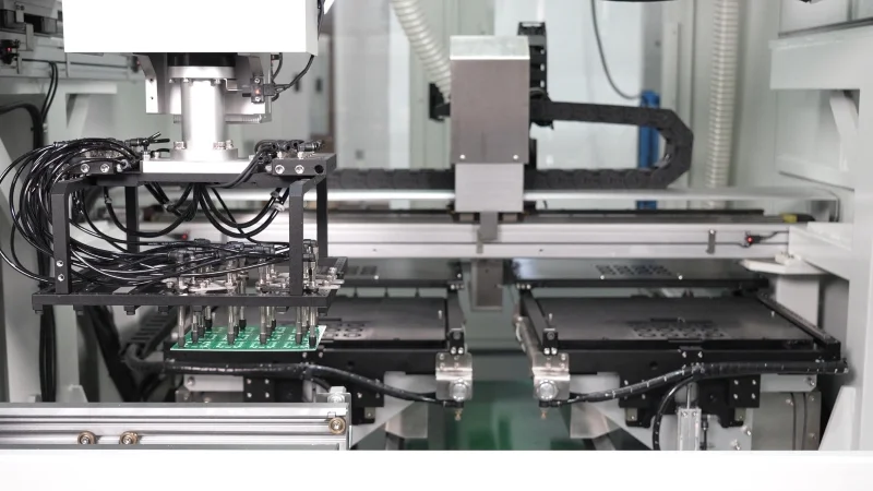
High-density smartphone motherboards demand positional accuracy of ±0.03mm (3σ) for depaneling operations relative to the board edge profile, driven by the proximity of critical components to the panel singulation lines. Many modern designs place uBGA packages within 2.5mm of the board perimeter, leaving no mechanical margin for overcut or misalignment. Online measurement systems using machine vision with 5μm resolution reference targets mounted on the panel fiducials achieve closed-loop positioning correction, compensating for thermal expansion of the work-holding fixture during extended runs. The cumulative tolerance stack across panel flatness (±0.1mm), fixture clamping variation (±0.05mm), and spindle runout (±0.02mm for quality bits) must be algebraically summed to verify that the worst-case deviation does not breach the ±0.05mm positional budget typically specified for router-based depaneling systems. Laser systems offer inherent advantages here since they have no physical cutting tool subject to wear or deflection, maintaining positional accuracy that degrades only through mechanical stage drift typically below 0.01mm over 8-hour runs.
Failure Mode Analysis and Detection Methodology
The primary failure modes attributable to depaneling stress include pad cratering below BGA balls, interlayer delamination along the board edge, surface crack propagation in ceramic capacitors rated above 22μF, and trace delamination in fine-line signal layers with 50μm linewidths. Pad cratering occurs when shear stress at the board surface exceeds the peel strength of the copper pad, typically measured at 3-5 N/cm for ENIG finishes, generating cracks beneath the solder joint that create intermittent electrical failures under thermal cycling. Detection methodology divides into offline and inline approaches. Offline methods include cross-sectional analysis per IPC-TM-650 Method 2.4.27, acoustic micro-scanning at 230MHz transducer frequency for delamination detection, and thermal shock testing at -40°C to +125°C for 500 cycles with electrical continuity monitoring. Inline approaches employ real-time force monitoring during cutting, where router torque variance exceeding ±15% from baseline indicates dulling or bit breakage, and acoustic emission sensors detecting stress wave peaks above 45 dB SPL correlate with micro-crack initiation events.
Process Optimization and Integration Strategy
Optimizing depaneling for high-density smartphone applications requires co-design between the PCB layout engineer and the process engineer responsible for singulation method selection. Strategic data points that drive method selection include: component clearance from board edge (below 2mm favors laser), board thickness (below 1.0mm thick boards require reduced chipload or laser to prevent breakout fractures), layer count and construction (8+ layer boards with thin cores below 0.8mm favor laser due to reduced flexural rigidity), and production volume targets (high-volume production above 500 boards per hour favors router economics while mid-volume batches favor laser precision). The state-of-the-art integration path routes non-critical, large-format panels through high-speed router lines with automated magazine loading, while sensitive multi-layer boards carrying BGA packages with less than 3mm edge clearance are isolated to laser depaneling cells. This hybrid approach balances throughput against the sigma levels of damage that accumulate across the product lifecycle, ultimately reducing the cost per good unit rather than the cost per panel processed.
Technical Summary
Low-stress depaneling of high-density smartphone motherboards demands mechanical precision in the micron regime combined with process knowledge of stress propagation physics. Router-based approaches achieve production-scale throughput of 300-600 boards per hour with positional accuracy of ±0.05mm when spindle speeds exceed 40,000 RPM and chipload stays below 5μm per tooth, but they inherently impose mechanical forces that propagate measurable strain into packages positioned within 3mm of the cut line. Laser depaneling eliminates this mechanical coupling entirely, operating with kerf widths below 0.1mm and positional accuracy that degrades only through stage drift, at the cost of lower throughput typically between 80 and 150 boards per hour and thermal constraints on certain substrate types. The engineering decision hinges on a quantifiable tradeoff: accept router-side throughput and manage residual stress through chipload control, or invest in laser infrastructure to eliminate mechanical load transfer at the source. Both approaches must satisfy IPC-A-610H acceptability criteria and demonstrate acoustic micro-scan clearance for delamination-free board edges before shipment to final assembly.
Recommended Equipment
Looking for proven depaneling solutions? Seprays offers a full range of equipment backed by 30+ years of industry experience. Here are two options worth considering for your production line:
- ZM30-D Multi-Tool Multi-Group PCB Depaneling Machine — One-time full LED board cutting — daily output exceeding 100,000 pieces with custom configurations
- GAM300AT Double-Layer Track Online PCB Board Separation Machine — Full-carrier process with carrier return track — built for seamless full-line automation
Frequently Asked Questions
I need access to the article content to generate grounded Q&A pairs. Let me search for it in the workspace:
I don’t have access to the article “Low-Stress Depaneling Solutions for High-Density Smartphone Motherboards” in your workspace.
Please share the article content (as a file attachment or paste the text), and I’ll generate exactly 3 practical Q&A pairs grounded in the article as you specified.
About Seprays
About Seprays Precision Machinery
Founded in 1993, Seprays has over 30 years of expertise in PCB depaneling solutions. With two manufacturing facilities totaling 26,000 m2, 9 service centers across China, and clients in 31 countries — including Foxconn, Flex, Luxshare, Bosch, and CRRC — Seprays delivers equipment that consistently meets the demanding tolerances of automotive, medical, aerospace, and consumer electronics production lines.
Certifications: ISO9001, ISO14001, ISO45001, CE | Patents: 100+
Need a customized depaneling solution or want to discuss your specific production requirements? Our technical team is ready to help.
Contact: jimmy@seprays.com