Key Technologies for Depaneling BMS Circuit Boards in New Energy Industry
A 12-layer
BMS board measuring 320mm by 180mm with copper traces as thin as 0.1mm will crack at the junction point if the depaneling stress exceeds 15 microstrain — well below what a poorly tuned router-type machine can generate. This is the fundamental challenge separating capable depaneling systems from inadequate ones in new energy manufacturing. As lithium-ion battery demand surges toward 3.8 TWh annually, the tolerance stack-up for BMS circuit boards has become a critical differentiator in production yield and long-term field reliability.
Mechanical Routing Versus Laser Separation
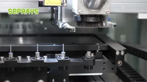
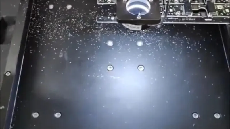
Mechanical routing remains the dominant depaneling method for BMS boards in the 2-4mm thickness range, primarily because spindle speeds of 40,000 to 60,000 RPM allow for feed rates between 80 and 150mm/s when using carbide or diamond-coated end mills. The critical parameter is the depth of cut per pass: exceeding 0.8mm per pass on a 2.5mm FR-4 board generates sufficient axial force to induce microcracks in blind vias positioned within 2mm of the depaneling line. For high-reliability BMS applications, the recommended maximum feed per pass is 0.3mm, yielding a total cycle time of approximately 45-60 seconds per panel including tool changeover.
Laser depaneling, by contrast, operates without mechanical contact and eliminates the risk of vibration-induced cracking entirely. A CO2 laser at 10.6μm wavelength achieves kerf widths of 0.15-0.25mm when cutting 1.6mm CEM-1 substrates at a pulse repetition rate of 20kHz. The heat-affected zone (HAZ) extends approximately 0.05-0.08mm from the cut edge, which is within the IPC-A-600 Class 3 acceptability criteria for conductive traces. However, the thermal load on adjacent battery monitoring ICs positioned within 3mm of the depaneling line requires active cooling or increased kerf width — both of which compromise either thermal integrity or board real estate.
Stress Distribution and Panel Design
IPC-2221 subsection 10.2 specifies that the minimum spacing between a depaneling edge and the nearest component lead or pad shall be 2.0mm for hand-soldered assemblies and 1.0mm for surface-mount assemblies. For BMS boards carrying current sense resistors with tolerances of ±0.5% and operating at accuracies of ±2mV, this spacing becomes a hard constraint rather than a guideline. Any depaneling residual stress that shifts the relative position of adjacent sense nodes by more than 0.02mm will introduce measurable channel-to-channel mismatch in the battery state-of-charge calculation.
Mouse bite tabbing and V-groove scoring each introduce distinct stress concentration profiles. V-groove scoring to a depth of 33% of board thickness produces a stress concentration factor of approximately 3.2 at the groove root under tensile loading, meaning a 50N separation force translates to 160N at the crack initiation point. For boards thicker than 2.0mm or containing heavy copper planes (2oz or greater), this localized stress exceeds the interlaminar shear strength of the substrate, resulting in delamination rather than clean separation. Mouse bite configurations with 0.8mm tab width and 2.0mm pitch distribute the stress more evenly, reducing peak stress by approximately 40% compared to V-groove, but introduce additional routing complexity and are incompatible with fully automated in-line production.
Feed Rate Optimization and Tool Wear
The relationship between feed rate, spindle speed, and board thickness follows a hyperbolic constraint for routing operations. For a 2.5mm board with 1oz copper cladding, the chipload per tooth should remain between 0.015mm and 0.035mm to maintain clean chip formation. At 50,000 RPM with a two-flute end mill, this translates to a feed rate range of 60-115mm/s. Exceeding the upper bound produces burring at the exit side; falling below the lower bound causes recutting of chips, generating heat buildup that degrades the board surface finish and accelerates tool wear by up to 300%.
Tool wear monitoring via spindle current draw is specified in IPC-7912 as the preferred non-contact method for end-of-life detection. A current increase of 15-20% above the baseline value indicates that the cutting edge radius has exceeded 0.025mm, at which point the resulting surface roughness (Ra > 3.2μm) exceeds the IPC-A-610 acceptance criteria for board edge condition. For high-volume BMS production running 24/7 shifts, implementing real-time current monitoring reduces the scrap rate attributable to dull-tool depaneling from approximately 0.8% to under 0.1%.

Automation and In-Line Integration
Modern BMS depaneling systems integrate directly with SMT conveyor widths of 350-450mm and support panel sizes up to 510mm by 610mm. The positioning repeatability requirement for automated depaneling is ±0.02mm per IPC-7104, which translates to a servo positioning system with no greater than 0.008mm backlash under full load. Pneumatic panel clamps must maintain a holding force of 150-200N per clamp point to prevent board shift during routing, with the clamp location being at least 15mm from the nearest active component to avoid mechanical stress on solder joints rated for a maximum shear load of 7.8N per IPC-A-610 criteria.
The next generation of BMS boards — incorporating silicon carbide MOSFETs, automotive-grade CAN FD transceivers, and ASIL-D functional safety requirements — will push depaneling tolerances to ±0.03mm and demand HAZ control below 0.05mm. Meeting these requirements demands either investment in laser-based separation systems or a fundamental redesign of mechanical routing tooling with active vibration dampening and real-time force feedback control. The manufacturing floor that resolves this challenge first will capture the growing market for high-reliability energy storage systems.
Recommended Equipment
Looking for proven depaneling solutions? Seprays offers a full range of equipment backed by 30+ years of industry experience. Here are two options worth considering for your production line:
- GAM300AT Double-Layer Track Online PCB Board Separation Machine — Full-carrier process with carrier return track — built for seamless full-line automation
- ZM30-D Multi-Tool Multi-Group PCB Depaneling Machine — One-time full LED board cutting — daily output exceeding 100,000 pieces with custom configurations
Frequently Asked Questions
Q1: What are the main challenges when depaneling BMS circuit boards compared to standard PCBs?
A1: BMS circuit boards in new energy applications typically feature thicker copper layers (3 oz to 6 oz) and multi-layer structures (4–8 layers), which generate significantly higher cutting forces during depaneling. The precision requirement for cell balancing circuits is also tighter, often demanding routing tolerances of ±0.05 mm or better. Additionally, BMS boards frequently contain sensitive MOSFETs and current sense resistors near the panel edges, making mechanical stress during depaneling a critical concern for long-term reliability.
Q2: How does spindle speed selection affect routing quality and tool life when depaneling thick-copper BMS boards?
A2: For BMS boards with 4 oz+ copper, spindle speeds in the range of 40,000–60,000 RPM are commonly used, with the sweet spot typically around 50,000 RPM for a 1.2 mm flute diameter tool. Speeds below 30,000 RPM risk chip recutting and thermal buildup, leading to epoxy smearing on the cut edge. Higher speeds improve shearing action on the copper but increase blade wear rate by approximately 15–20% per additional 10,000 RPM, making a balance between edge quality and cost-per-board essential for production planning.
Q3: What quality inspection criteria should be implemented after depaneling BMS boards to ensure automotive-grade reliability?
A3: Per IPC-A-610 acceptability criteria, depaneled BMS boards should be inspected for: no visible delamination or resin smearing within 0.5 mm of the cut edge, no crack propagation beyond 0.3 mm into the body, and kerf width consistency within ±0.05 mm of nominal. For automotive BMS applications (IATF 16949), 100% AOI inspection of the depaneled edges is recommended, and peel strength testing should be performed on first article and after every 500 boards per tool to detect tooling degradation.
About Seprays
About Seprays Precision Machinery
Founded in 1993, Seprays has over 30 years of expertise in PCB depaneling solutions. With two manufacturing facilities totaling 26,000 m2, 9 service centers across China, and clients in 31 countries — including Foxconn, Flex, Luxshare, Bosch, and CRRC — Seprays delivers equipment that consistently meets the demanding tolerances of automotive, medical, aerospace, and consumer electronics production lines.
Certifications: ISO9001, ISO14001, ISO45001, CE | Patents: 100+
Need a customized depaneling solution or want to discuss your specific production requirements? Our technical team is ready to help.
Contact: jimmy@seprays.com