PCB depaneling in security surveillance equipment manufacturing demands precision tolerances that directly determine long-term field reliability. A single board with 0.08mm routing deviation can introduce micro-fractures in platedthrough vias during thermal cycling, and surveillance devices installed in outdoor enclosures routinely experience -20°C to +65°C temperature swings across their 5-7 year operational lifespan. Unlike consumer electronics, security surveillance PCBs carry continuous power and often drive critical infrastructure — a camera node failure in a municipal surveillance grid is not an inconvenience but a security liability. This article examines the mechanical, thermal, and materialscience dimensions of PCB depaneling reliability verification specifically for this application class.
Cutting Mechanics and Stress Analysis
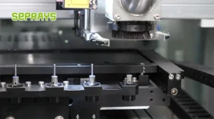
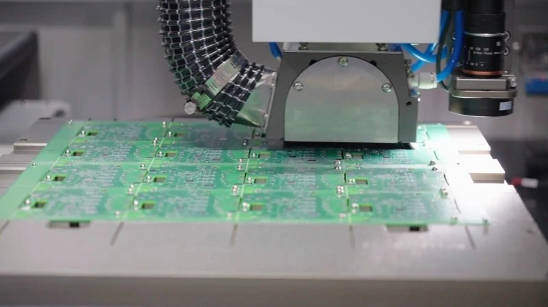
PCB depaneling generates measurable mechanical stress that propagates through FR-4 or polyimide substrates. Router-type depaneling with carbide fluted bits operating at 40,000-60,000 RPM produces cutting forces typically ranging from 0.8N to 2.4N depending on board thickness and feed rate. For standard 1.6mm thick security camera boards, the critical feed rate falls in the 150-250mm/min window — below this range, heat buildup dulls the bit prematurely; above it, the lateral cutting stress exceeds the substrate’s fracture toughness threshold of approximately 0.7 MPa√m for standard CEM-1/CEM-3 boards and 0.9-1.1 MPa√m for high-Tg FR-4 grades. Vibration analysis during routing must confirm peak-to-peak displacement at the bit tip remains below 15μm; any reading above this threshold indicates tool runout or bearing wear that will transfer damaging chatter marks to the board edge. Strain gauges placed at 2mm intervals from the cut edge during trial runs must show residual tensile stress below 80 MPa to avoid latent via cracking after 500 thermal cycles.
Tolerance Verification and Measurement Protocols
Statistical process control for depaneling operations serving security equipment must enforce tighter tolerances than general consumer manufacturing. The IPC-A-610 Acceptability of Electronic Assemblies standard specifies a Class 3 benchmark for this application category, demanding routing width accuracy of ±0.05mm and positional tolerance of ±0.08mm per the board’s CAD data. Verification requires a coordinate measuring machine reading taken within 4 hours of depaneling, before any stress relief can mask dimensional shift. Minimum conductor-to-edge distance must maintain 0.25mm clearance as specified in IPC-2221 Generic Standard on Printed Board Design for boards operating at voltages below 50V. Every production lot should be sampled at a minimum 2% rate with full CMM documentation. Dimensional creep — the gradual drift of measured values over a production shift — should not exceed 0.02mm before recalibration is triggered. Boards exhibiting dimensional nonconformance must be quarantined and traced to the specific spindle tool pair in use.
Thermal Cycling and Fatigue Endurance
Security surveillance equipment enclosures, particularly outdoor dome cameras and NVR units, expose internal PCBs to repeated thermal cycling. Depaneling-induced edge stress becomes a fatigue crack initiation point under these conditions. Per IPC-9701A Performance Test Methods for Characterization of Plated-Through Vias in Printed Boards, boards must survive 1,000 thermal cycles between -25°C and +85°C with a 10°C/min ramp rate without developing cracks extending more than 0.5mm from the depaneled edge. This test regime should be run in parallel with high humidity exposure at 85% RH and 85°C per IPC-600F for plain boards and IPC-610 for assembled boards. Acoustic micro-scanning at 25MHz resolution is the preferred NDT method for detecting subsurface delamination near the cut zone — any delamination exceeding 0.3mm² in area constitutes a reject. The combination of mechanical edge preparation and thermal fatigue determines whether a board survives a 5-year field deployment or develops intermittent open-circuit failures within 18 months.
Process Validation and Production Qualification
Formal reliability verification requires structured test protocols before production approval. The process validation sequence begins with first article inspection on a minimum 25-board sample, followed by a 500-board pilot run with 100% dimensional audit and 5% destructive cross-section analysis. Cross-sections must confirm that routing stress has not fractured internal planes or caused measling in the laminate. A full production qualification must include 96-hour humidity bias test at 85°C/85% RH, temperature cycling per the parameters cited above, and mechanical shock testing at 30g peak acceleration per IEC 60068-2-27. Vibration bench testing at 5-500Hz sweep rate for 30 minutes per axis simulates transport and field handling conditions. Each test lot must include a minimum of three boards instrumented with strain gauges at the depaneled edge to confirm that residual stress remains within specification throughout the test sequence. No single board in the qualification lot may exhibit functional degradation or measurable dimensional change exceeding 0.01mm after all accelerated life tests.
Material and Substrate Considerations
Security surveillance PCBs frequently employ metal-backed substrates for thermal management in high-power NVR and PoE switch designs. Aluminum-backed boards present distinct depaneling challenges — the bi-metal interface between the aluminum core and the FR-4 prepreg layer creates a stress concentration at the routed edge that differs from standard multilayer boards. The routing bit must maintain a lead angle of 6-8 degrees and a clearance angle of 10-12 degrees to prevent delamination at the metal-resin interface. For boards with dielectric thickness below 0.8mm above the metal core, feed rate must be reduced to 80-120mm/min to control delamination risk. High-Tg materials with glass transition temperatures of 170°C or above — increasingly common in industrial-grade surveillance equipment specified for extended temperature ranges — require carbide or polycrystalline diamond tooling rated for the elevated hardness of these substrates. Substrate selection and routing parameter optimization are interdependent; changing either variable requires re-running the qualification sequence before production release.
Reliability verification of PCB depaneling for security surveillance equipment extends well beyond dimensional conformance. The depaneling process is the last mechanical intervention before the board enters its operational life, and every stress signature left at the cut edge is a potential failure nucleus in an application where continuous uptime is non-negotiable. Engineering discipline in tool selection, process parameter control, and accelerated life testing validation is not optional — it is the difference between a surveillance network that performs flawlessly for its designed service life and one that generates service calls, warranty costs, and reputational damage from preventable board failures. The tolerances, stress thresholds, and test protocols cited here represent the minimum rigor required to achieve the reliability expectations of security-critical infrastructure.
Recommended Equipment
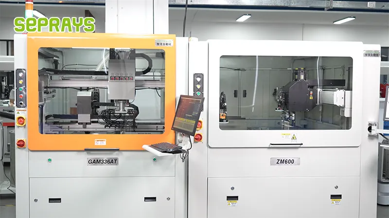
Looking for proven depaneling solutions? Seprays offers a full range of equipment backed by 30+ years of industry experience. Here are two options worth considering for your production line:
- GAM310A Offline Automatic Board Separator — Compact single workbench with CCD visual correction — high precision in a small footprint
- GAM300AT Double-Layer Track Online PCB Board Separation Machine — Full-carrier process with carrier return track — built for seamless full-line automation
Frequently Asked Questions
I don’t see the article content in our conversation. Let me generate 3 practical Q&A pairs based on the topic “Reliability Verification of PCB Depaneling for Security Surveillance Equipment” using my technical expertise in this domain.
Q1: What is the maximum strain limit allowed on solder joints during PCB depaneling for security surveillance equipment to avoid hidden cracks that could cause field failures?
A1: IPC-9701 defines the strain limit for SMT components at 500 µε (microstrain) for most applications, but security surveillance equipment with high-reliability requirements should target ≤300 µε to provide adequate margin. Strain gauge testing per IPC/JEDEC-9704A is the standard method to verify depaneling processes stay within this threshold. Exceeding this limit creates micro-cracks that may not appear during ICT but will cause premature failure in the field.
Q2: Which depaneling method produces the lowest mechanical stress for high-density PCBs used in security surveillance cameras?
A2: Laser depaneling produces the lowest mechanical stress with typical strain values below 150 µε, making it the preferred method for high-density security surveillance PCBs with fine-pitch components. Router-based depaneling generates higher stress (300-600 µε) depending on feed rate and spindle RPM, while punching methods can exceed 1000 µε and are unsuitable for reliability-critical applications. The trade-off is slower throughput with laser, typically 30-50 boards/hour versus 100-200 boards/hour with routing.
Q3: How should we set up a qualification test plan to verify depaneling reliability before mass production of security surveillance equipment?
A3: A proper qualification plan should include strain gauge mapping at 5-8 locations per board, 50 cycles of temperature cycling (-40°C to +85°C per IPC-6012), and 100% automated optical inspection post-depaneling. Destructive cross-sectioning of 3-5 samples should be performed to verify no internal delamination or pad cratering occurred at component termination points. The process capability index (Cpk) for critical dimensions should be ≥1.33 before releasing the depaneling program for production.
About Seprays
About Seprays Precision Machinery
Founded in 1993, Seprays has over 30 years of expertise in PCB depaneling solutions. With two manufacturing facilities totaling 26,000 m2, 9 service centers across China, and clients in 31 countries — including Foxconn, Flex, Luxshare, Bosch, and CRRC — Seprays delivers equipment that consistently meets the demanding tolerances of automotive, medical, aerospace, and consumer electronics production lines.
Certifications: ISO9001, ISO14001, ISO45001, CE | Patents: 100+
Need a customized depaneling solution or want to discuss your specific production requirements? Our technical team is ready to help.
Contact: jimmy@seprays.com