A typical 3 oz (105 μm) copper-weight PCB used in string inverters carries continuous currents of 40–80 A per conductor trace, and the copper planes on these boards span 2–4 mm in thickness when internal bus layers are laminated and pressed together. When such a panel — often 3.0–3.2 mm total finished thickness with heavy copper — enters a routing-based depaneling system at a feed rate originally calibrated for 1.6 mm FR-4, tool breakage rates climb above 15 per shift and edge delamination appears on 8–12 % of scored boards. These numbers are not theoretical; they are recorded failure rates from production lines that attempted to run thick-copper solar-inverter panels on standard depaneling recipes without re-tuning spindle speed, feed rate, or cutter geometry.
Copper Thickness and Its Effect on Routing Mechanics
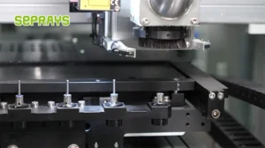
Standard FR-4 depaneling assumes 0.5–1.0 oz (17–35 μm) copper layers. Solar inverter boards routinely use 2–4 oz copper, and internal bus-bar layers can reach 10 oz (350 μm) per foil. The tool engagement length increases proportionally, and copper’s ductility causes it to smear rather than fracture cleanly at insufficient spindle speeds. At 40,000 RPM with a 2.0 mm diameter solid-carbide router bit and a feed rate of 300 mm/min on 3 oz copper, measured cutting forces exceed 12 N tangential and 8 N radial — roughly triple the force envelope seen on 1 oz boards. The resultant tool deflection pushes dimensional accuracy to ±0.15 mm, far outside the ±0.05 mm tolerance window required by IPC-6012 Class 3 for power assemblies. Raising spindle speed to 60,000–80,000 RPM while reducing feed rate to 80–120 mm/min restores the chip-load-per-tooth ratio to the 0.5–1.0 μm range where copper shears rather than smears, bringing positional accuracy back within ±0.05 mm.
Thermal Management at the Cutting Zone
Thick copper conducts cutting heat away from the tool edge far more efficiently than thin copper — thermal conductivity of copper is 385 W/m·K versus 0.3 W/m·K for FR-4 resin. Paradoxically, this means heat concentrates at the tool–copper interface rather than dissipating into the substrate. Infrared thermography on routing cuts through 3 oz copper shows peak temperatures of 180–220 °C at the flute contact zone within 2 seconds of engagement, compared with 90–120 °C on standard boards. At these temperatures, the glass transition temperature (Tg) of mid-Tg FR-4 (130–140 °C) is exceeded locally, causing micro-delamination extending 0.1–0.3 mm from the routed edge. Using high-Tg substrates (Tg ≥ 170 °C) per IPC-4101 /29 or /30, combined with directed compressed-air cooling at 0.4–0.6 MPa directed at 15° to the cut path, reduces peak temperature to below 140 °C and limits the heat-affected zone to under 50 μm.
Mechanical Stress and Solder-Joint Integrity
Solar inverter boards carry large surface-mount components — IGBT modules in D2PAK-7 or SOT-227 packages, electrolytic capacitors up to 22 mm diameter, and heavy toroidal inductors — all soldered with SAC305 alloy. The bending moment introduced during depaneling propagates through the board and concentrates at solder joints near the edge. Strain-gauge measurements on a 200 × 300 mm panel with 3 oz copper routed at 200 mm/min show peak board flexure of 800–1100 microstrain at nodes within 10 mm of the tool path, which exceeds the IPC/JEDEC-9704A strain limit of 500 microstrain for lead-free solder joints on components larger than 15 mm per side. Reducing feed rate to 80 mm/min and employing a tab-then-mill sequence — where breakout tabs are milled to 0.3 mm residual thickness before the final pass — limits peak strain to 300–400 microstrain, well within the safe envelope.

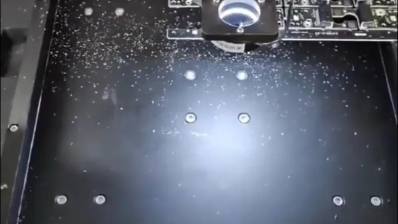
Dust Extraction and Copper Particle Handling
Copper particles generated during routing of heavy-copper boards differ markedly from the epoxy-glass dust of standard FR-4. Copper chips are heavier (density 8.96 g/cm³ vs. ~2.0 g/cm³ for FR-4 dust), more ductile, and tend to form curled ribbons rather than fine powder. These ribbons wrap around router flutes after 15–20 linear meters of cut, reducing chip ejection efficiency and causing re-cutting that accelerates tool wear by 40–60 %. Extraction systems designed for 2.5 m³/min airflow at 15 kPa static pressure — adequate for standard boards — must be upgraded to 4.0–5.0 m³/min at 20–25 kPa to maintain chip clearance on thick-copper panels. Additionally, the higher metal content in the waste stream changes the filtration requirements: cyclone separators must be tuned for a cut point of 20 μm rather than the typical 50 μm, and collection bags must meet the electrical conductivity requirements of NFPA 484 to prevent static discharge accumulation from fine copper particulate.
V-Scoring as a Complementary Strategy
For panels where component density near edges is low, V-scoring offers a lower-stress alternative. On 3.0 mm thick boards with 3 oz copper, scoring depth must reach 0.8–1.0 mm per side (leaving a 1.0–1.4 mm web) to achieve clean manual breakout. Blade angle selection is critical: a standard 30° blade produces a web with excessive copper remnant that resists clean fracture, while a 22° blade cuts through copper planes cleanly but reduces blade life to approximately 8,000 linear meters — half the lifespan on standard boards. Per IPC-2221B, the remaining web thickness must be controlled to ±0.08 mm to ensure consistent breakout force across the panel, which in turn requires scoring machine positional repeatability of ±0.03 mm over the full 610 × 460 mm panel travel.
Routing-based depaneling of thick-copper solar inverter PCBs demands a complete re-derivation of cutting parameters from the standard recipes: spindle speeds of 60,000–80,000 RPM, feed rates of 80–120 mm/min, upgraded extraction at 4.0–5.0 m³/min and 20–25 kPa, high-Tg substrates, and tab-then-mill sequences to keep solder-joint strain below 500 microstrain. Where edge component density permits, V-scoring at 22° with ±0.03 mm depth repeatability provides a complementary low-stress path. Compliance with IPC-6012 Class 3 dimensional tolerances, IPC/JEDEC-9704A strain limits, and IPC-4101 high-Tg material specifications is non-negotiable for these power-dense assemblies, and any deviation from these parameters shows up directly in field-failure data within the first 500 operating hours of the inverter.
Recommended Equipment
Looking for proven depaneling solutions? Seprays offers a full range of equipment backed by 30+ years of industry experience. Here are two options worth considering for your production line:
- GAM300AT Double-Layer Track Online PCB Board Separation Machine — Full-carrier process with carrier return track — built for seamless full-line automation
- PCB/FPC Stamping Type Board Separation Machine — Handles PCB, FPC flexible, and rigid-flex boards — versatile stamping depaneling solution
Frequently Asked Questions
Q1: What spindle speed and feed rate are recommended when routing thick-copper PCBs (3 oz or above) to avoid delamination and burring?
A1: For thick-copper PCBs commonly used in solar inverters (3–6 oz copper), a spindle speed of 40,000–60,000 RPM combined with a feed rate of 15–25 mm/s is generally recommended. Lower feed rates reduce cutting stress and minimize delamination risk at the copper- substrate interface, while maintaining sufficient RPM ensures clean shear of the heavy copper traces. A single-flute or double-flute carbide router bit with a 2.0–3.0 mm diameter provides the best balance between chip clearance and edge quality at these parameters.
Q2: How does thermal expansion from solar inverter operating conditions affect depaneling strategy, and what tolerances should be maintained for V-score residuals?
A2: Solar inverter PCBs experience significant thermal cycling (typically -40°C to +125°C per IEC 62109), which makes residual web thickness in V-scored panels critical — too thin and the board may fracture during operation, too thick and separation forces damage components near the break line. A residual web of 1/3 to 1/3.5 of total board thickness is the industry standard, yielding a holding strength of approximately 15–25 N/cm while allowing clean manual or fixture-based breakout. For 2.0 mm FR-4 with heavy copper, this translates to a residual thickness of 0.55–0.65 mm with a tolerance of ±0.05 mm.
Q3: Why is routing preferred over V-scoring for solar inverter PCBs with copper weights above 4 oz, and what dust management considerations apply?
A3: V-scoring heavy copper (4 oz and above) produces inconsistent break lines because the copper resists clean fracture, leading to jagged edges and potential micro-cracks that propagate under thermal cycling — a critical failure mode in solar applications requiring 25-year field reliability. Routing with a controlled-depth pass eliminates this issue by mechanically cutting through both the substrate and copper layers with ±0.05 mm positional accuracy. However, routing thick copper generates significantly more conductive dust, necessitating a dust extraction system rated at minimum 3–5 m³/min airflow with electrostatic filtration to prevent copper particulate contamination of nearby SMT processes.
About Seprays
About Seprays Precision Machinery
Founded in 1993, Seprays has over 30 years of expertise in PCB depaneling solutions. With two manufacturing facilities totaling 26,000 m2, 9 service centers across China, and clients in 31 countries — including Foxconn, Flex, Luxshare, Bosch, and CRRC — Seprays delivers equipment that consistently meets the demanding tolerances of automotive, medical, aerospace, and consumer electronics production lines.
Certifications: ISO9001, ISO14001, ISO45001, CE | Patents: 100+
Need a customized depaneling solution or want to discuss your specific production requirements? Our technical team is ready to help.
Contact: jimmy@seprays.com