Semiconductor test boards require particle contamination levels below 0.5 mg per panel after depaneling—a threshold 10× stricter than standard consumer electronics PCB processing. At advanced packaging facilities handling probe cards and load boards for wafer testing, a single conductive particle measuring 10–50 μm can cause probe tip shorts, costing $15,000–$50,000 per test head incident and 4–8 hours of unplanned downtime for cleaning and recalibration.
Cleanliness Classification and Particle Limits
Semiconductor test boards fall into IPC-5704 cleanliness Class 3 or higher, specifying maximum residual particle counts per unit area. For test boards with probe contact densities exceeding 400 tips per square centimeter, the acceptable particle density drops to <5 particles/cm² for particles ≥25 μm. Standard FR-4 depaneling typically tolerates 50–100 particles/cm² at the same particle size threshold. This 10–20× difference drives fundamental equipment selection: router-based systems with integrated vacuum extraction achieving 95–98% chip capture rates versus laser systems that vaporize material and eliminate particulate generation entirely. Ultrasonic depaneling, while generating minimal mechanical debris, produces sub-micron slurry particles that require additional DI water rinsing and cleanroom-compatible drying processes.
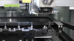
Router Spindle Sealing and Dust Extraction Efficiency
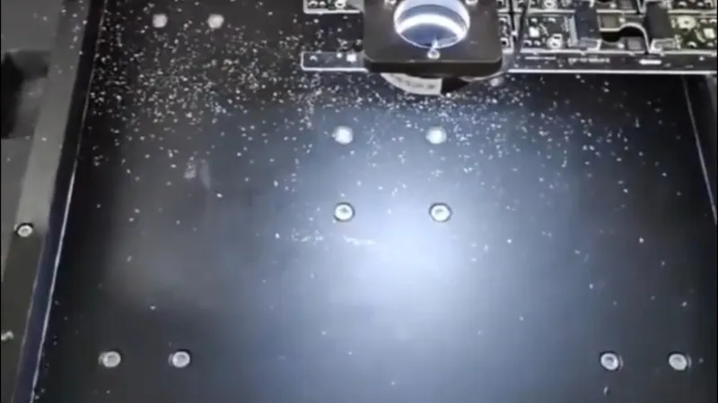
High-cleanliness depaneling routers employ sealed spindle bearings with IP54 or IP65 ingress protection ratings, preventing lubricant migration into the cutting zone. Standard spindles operating at 40,000–60,000 RPM with open bearing designs can aerosolize bearing grease, depositing hydrocarbon films on copper pads at concentrations of 0.1–0.3 μg/cm²—sufficient to increase contact resistance by 15–25% on fine-pitch probe interfaces. Sealed spindles with ceramic hybrid bearings (Si3N4 balls, steel races) eliminate this contamination pathway while supporting continuous operation at 60,000–80,000 RPM with radial runout below 2 μm. The vacuum extraction system must maintain 80–120 CFM airflow at the cutting point with static pressure ≥8 inches H2O, positioned 3–5 mm from the tool tip to capture debris before it disperses. Extraction nozzle geometry matters: concentric annular designs achieve 92–96% capture efficiency versus 75–85% for single-port side extraction.
Material Selection for Low-Debris Cutting
Tool material and geometry directly control chip formation and particle size distribution. For semiconductor test boards using high-Tg FR-4 (Tg ≥170°C) or polyimide substrates with thicknesses of 1.6–3.2 mm, single-flute upcut router bits with 0.8–1.2 mm flute length produce continuous helical chips averaging 0.3–0.8 mm length, which vacuum systems capture efficiently. Downcut geometries force chips into the kerf, increasing re-cutting and generating 5–10× more fine particles (<50 μm). Tungsten carbide tools with AlTiN or diamond-like carbon (DLC) coatings maintain cutting edge radius below 8 μm for the first 500–800 linear meters of cutting, after which edge degradation increases burr height from <0.05 mm to 0.1–0.2 mm and fine particle generation by 40–60%. Tool life monitoring via spindle load current (±5% threshold) enables predictive replacement before contamination escalation.

Static Charge Control and Particle Adhesion
Depaneling routers generate electrostatic charges of 5–15 kV on panel surfaces through friction and chip ejection, causing sub-50 μm particles to adhere with forces exceeding gravitational settling by 100–1000×. Ionized air systems integrated into extraction nozzles, delivering ±10V balanced output at 50–100 L/min flow rate, neutralize surface charges within 2–4 seconds of panel exit from the cutting zone. Without ionization, post-depaneling particle counts on vertical surfaces remain 3–5× higher than horizontal surfaces even with identical extraction airflow. Conductive tooling plates with grounded contact points (surface resistance <10⁶ Ω/sq) provide additional charge dissipation paths. Cleanroom-compatible depaneling systems (ISO Class 6–7) incorporate HEPA-filtered (99.97% at 0.3 μm) exhaust air recirculation, preventing re-entrainment of captured particles into the work envelope.
Post-Process Verification and Quality Metrics
Semiconductor test board cleanliness verification requires quantitative measurement beyond visual inspection. Ionic contamination testers measuring surface conductivity per IPC-TM-650 method 2.3.25 detect flux and lubricant residues at concentrations as low as 0.1 μg NaCl equivalent per cm². Particle counting using scattered light sensors (ISO 14644-1 compliant) with 0.5 μm lower detection threshold provides statistical process control data. For high-reliability applications, SEM-EDX analysis of random particle samples identifies composition—copper particles indicate tool wear or excessive feed rates; epoxy-glass particles suggest suboptimal cutting parameters; organic contamination points to bearing seal degradation. Cleanliness audit trails linking depaneling batch numbers to particle count distributions enable root cause analysis when test failures correlate with specific panel lots.
Semiconductor test board depaneling demands integrated contamination control across spindle sealing, tool geometry, extraction efficiency, static neutralization, and quantitative verification—each parameter contributing to the 10–20× cleanliness improvement over standard PCB processing. The economic justification is clear: preventing a single particle-induced test head failure saves more than the annual operating cost differential between standard and cleanroom-compatible depaneling equipment, making high-cleanliness specifications a process necessity rather than an optional upgrade for facilities handling advanced probe cards and high-density test interfaces.
Recommended Equipment
Looking for proven depaneling solutions? Seprays offers a full range of equipment backed by 30+ years of industry experience. Here are two options worth considering for your production line:
- GAM310A Offline Automatic Board Separator — Compact single workbench with CCD visual correction — high precision in a small footprint
- GAM300AT Double-Layer Track Online PCB Board Separation Machine — Full-carrier process with carrier return track — built for seamless full-line automation
Frequently Asked Questions
Q1: What is the maximum allowable particulate contamination level on semiconductor test boards after the depaneling process?
A1: For semiconductor test boards, particulate contamination must be controlled to less than 100 particles per square foot for particles ≥ 0.5μm, with strict Class ISO 5 (Class 100) cleanroom standards applied during depaneling. Any conductive debris exceeding 50μm in size poses a risk of short circuits and must be eliminated through optimized dust extraction systems operating at ≥15 m/s airflow velocity.
Q2: Which depaneling method produces the lowest particulate contamination for high-density semiconductor test boards with sensitive components?
A2: Laser depaneling produces the cleanest cut with minimal particulate generation, typically generating less than 5mg of debris per meter of cut length compared to 50-100mg for mechanical routing. When laser systems are not feasible, dedicated PCB router systems with integrated high-efficiency HEPA filtration (99.99% efficiency at 0.3μm) and spindle speeds maintained between 30,000-40,000 RPM provide the next best alternative for contamination control.
Q3: How should manufacturers validate that depaneling processes meet cleanliness standards for semiconductor test board production?
A3: Implement a three-stage validation protocol: (1) post-depaneling visual inspection under 40x-100x magnification to detect particles ≥ 25μm, (2) ionic contamination testing per IPC-CH-65B standards with target values below 1.56 μg/cm² NaCl equivalent, and (3) functional testing of test boards in controlled environments to verify no latent defects from debris contamination, with statistical process control limits set at ±3σ from baseline measurements.
About Seprays
About Seprays Precision Machinery
Founded in 1993, Seprays has over 30 years of expertise in PCB depaneling solutions. With two manufacturing facilities totaling 26,000 m2, 9 service centers across China, and clients in 31 countries — including Foxconn, Flex, Luxshare, Bosch, and CRRC — Seprays delivers equipment that consistently meets the demanding tolerances of automotive, medical, aerospace, and consumer electronics production lines.
Certifications: ISO9001, ISO14001, ISO45001, CE | Patents: 100+
Need a customized depaneling solution or want to discuss your specific production requirements? Our technical team is ready to help.
Contact: jimmy@seprays.com