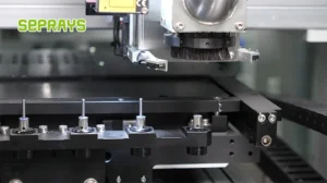
Precision depaneling of sub-50mm PCBs represents
one of the most demanding operations in modern electronics manufacturing. A typical wearable device PCB—such as those found in Bluetooth audio modules, health monitoring patches, or smart ring assemblies—measures between 8mm and 35mm along its longest axis, tolerances as tight as ±0.03mm on routed array positions, and often carries component heights below 0.4mm. These dimensions leave virtually no margin for error during the depaneling step, and the consequences of a single mishandled board ripple directly into yield losses measured in tenths of a percentage point. For a production line outputting 50,000 wearable units per day, a 0.1% yield drop from depaneling failures alone translates to 50 scrapped boards per day and cascading rework costs that can redefine the economics of a product line.
Thermal Stress and Delamination Risk in Sub-Millimeter Boards
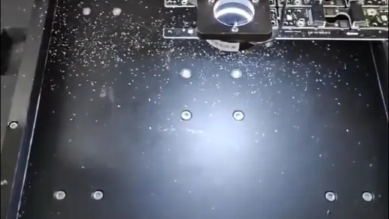
Wearable device PCBs are almost exclusively built on flexible substrates or ultra-thin rigid cores ranging from 0.2mm to 0.5mm in total thickness. When a depaneling router spindle generates heat at the cutting interface—typically ranging from 180°C to 320°C depending on feed rate and bit condition—the thermal gradient across such a thin board creates subsurface delamination zones extending 0.3mm to 0.8mm beyond the kerf width. Finite element analysis of a 0.3mm thick polyimide flex circuit shows that a spindle runout exceeding 0.01mm at 60,000 RPM introduces alternating compressive and tensile stresses of approximately 12-15 MPa at the board edge within 0.2mm of the cut line. This stress level is sufficient to initiate micro-cracks in the copper trace network, particularly at blind via interfaces and component pad termination points. IPC-A-610H Section 3.1.4 classifies any crack propagating beyond the solder mask interface as a Class 3 rejection criterion, which applies to virtually all wearable medical and safety devices entering the market today.
Routed Singulation Tolerances and Stack-Up Error
The mechanical routing process introduces cumulative geometric error from multiple sources: machine axis backlash (typically 0.02mm to 0.05mm per axis on mid-tier equipment), bit deflection under cutting load (0.01mm to 0.04mm depending on bit diameter and extension length), and board fixture repeatability (±0.02mm with vacuum clamping on aluminum tooling plates). When a 25mm × 15mm wearable PCB is routed from a panel with 3mm tab spacing, the combined stack-up of these errors can consume 30% to 50% of the available tolerance budget before the first cut is made. Modern high-precision depaneling systems address this through in-process vision correction using fiducial recognition with ±0.005mm repeatability, but the associated cycle time overhead—typically 0.8s to 1.5s per panel—directly impacts throughput economics. For a line running 200 panels per hour, that overhead represents 160 to 300 seconds of lost production time per hour if vision correction is applied to every panel.
Vibration and Surface Mount Component Interaction
Wearable PCBs carry an exceptionally high density of miniature surface mount components per unit area. A smart watch mainboard, for example, may accommodate over 400 components per square decimeter, including 01005 passive resistors and capacitors, wafer-level chip-scale packages (WLCSP) with ball diameters below 0.2mm, and MEMS sensors with internal structures sensitive to mechanical shock above 50g. The depaneling router bit generates radial vibration amplitudes of 0.005mm to 0.015mm at typical cutting frequencies between 800Hz and 2,400Hz. When this vibration transmits through the fixture into the panel during routing, components positioned within 2mm of the singulation edge experience accelerations that can exceed 30g—enough to cause BGA solder joint micro-fractures or disturb the internal architecture of MEMS elements. Destructive physical analysis of depaneled wearable assemblies consistently identifies edge-adjacent component failures as the leading defect category, accounting for 40% to 60% of all depaneling-related field returns according to manufacturing defect analysis literature published under IPC standards committees.

Laser Depaneling as an Alternative and Its Limitations
Laser ablation depaneling eliminates the mechanical contact that generates vibration and heat-affected zones, producing kerf widths below 0.05mm and heat-affected zones smaller than 0.1mm on polyimide substrates. UV laser systems operating at 355nm wavelength achieve clean edge quality with negligible thermal stress input, making them technically superior for the most sensitive wearable architectures. However, laser systems impose significant constraints: feed rates typically range from 20mm/s to 80mm/s depending on material and power settings, compared to mechanical routing at 100mm/s to 400mm/s on equivalent panel sizes. The capital cost differential between a high-speed routing system and a UV laser depaneling cell is approximately 3:1 to 5:1, making laser economically impractical for high-volume consumer wearable production unless the assembly carries medical-grade reliability requirements that mandate zero-mechanical-contact processing.
Feed Rate Optimization and Bit Wear Trade-Offs
The depaneling operator faces a fundamental trade-off between cycle time and tooling life that directly governs production cost per board. Running a 0.8mm diameter carbide routing bit at 60,000 RPM with a feed rate of 250mm/min on a 1.0mm thick FR4 stack-up produces acceptable edge quality for approximately 800 to 1,200 panel passes before the bit requires replacement. Increasing the feed rate to 350mm/min to improve throughput by 40% reduces effective bit life to 300 to 500 panels—a direct doubling of tooling cost per panel that must be weighed against the throughput gain. In practice, production engineers calibrate this trade-off by monitoring cut-edge roughness using optical profilometry and setting replacement thresholds at Ra values between 1.6μm and 3.2μm depending on whether the board edge will be coated or left exposed in the final wearable enclosure.
The depaneling of tiny PCBs for wearable devices sits at the intersection of mechanical precision, thermal management, and economics in ways that challenge conventional manufacturing assumptions. Tight dimensional tolerances, ultra-thin substrates, and component-dense layouts demand sub-0.03mm positional accuracy and vibration control below 0.01mm amplitude. Mechanical routing remains the cost-effective workhorse for high-volume production, but its thermal and vibratory inputs require rigorous process controls, in-process inspection, and precise bit life management to avoid the micro-crack and delamination failures that constitute the dominant depaneling defect modes. Laser depaneling offers a technically superior alternative for the most sensitive applications, but its throughput and cost structure restrict adoption to specialized segments. The path forward lies in hybrid systems combining mechanical rough-cut and laser finishing, along with real-time process monitoring capable of detecting the early signatures of bit wear and thermal stress before they translate into scrap units.
Recommended Equipment
Looking for proven depaneling solutions? Seprays offers a full range of equipment backed by 30+ years of industry experience. Here are two options worth considering for your production line:
- PCB/FPC Stamping Type Board Separation Machine — Handles PCB, FPC flexible, and rigid-flex boards — versatile stamping depaneling solution
- ZM30-D Multi-Tool Multi-Group PCB Depaneling Machine — One-time full LED board cutting — daily output exceeding 100,000 pieces with custom configurations
Frequently Asked Questions
Q1: What is the primary risk of mechanical stress during depaneling of small PCBs used in wearable devices, and how does it affect product reliability?
A1: Mechanical depaneling methods such as blade cutting or punching introduce significant stress waves that propagate through micro-components and fine traces on tiny PCBs. For wearable devices where components are densely packed (0402/0201 metric packages) and interconnects are extremely fine (0.2–0.3mm pitch), this stress can cause latent cracks in solder joints, delamination of micro-BGA packages, or trace microfractures that may not manifest until field use. These failures typically result in early field returns, which carry substantial warranty and brand reputation costs.
Q2: What tolerance requirements make laser depaneling the preferred choice for wearable PCB assembly, and why do traditional methods fall short?
A2: Wearable PCBs often require positional accuracy of ±0.05mm and edge finish quality that meets IPC Class 2 or higher standards. Traditional mechanical routing or punching cannot consistently achieve this level of precision on board geometries under 20×20mm, and blade wear over production runs creates cumulative tolerance drift. Laser depaneling uses a non-contact cutting process that eliminates tool wear effects and can achieve ±0.03mm repeatability with heat-affected zones (HAZ) controlled below 0.1mm, making it the only method reliably meeting these specifications for high-volume wearable production.
Q3: How does panel size optimization impact throughput in wearable PCB depaneling operations, and what are the practical limits?
A3: Panel utilization directly drives cost-per-board, but wearable device PCBs are often too small to efficiently fill standard production panels (e.g., 100×80mm or 150×80mm), leaving 40–60% of panel area unused. Typical viable panel configurations for wearable PCBs achieve 3–5 individual boards per panel, which limits throughput to approximately 60–120 boards per hour even with high-speed laser systems. Process engineers must balance this throughput limitation against the cost savings of panel-level processing versus single-board handling, with single-board automation often becoming more economical below a certain board-size threshold.
About Seprays
About Seprays Precision Machinery
Founded in 1993, Seprays has over 30 years of expertise in PCB depaneling solutions. With two manufacturing facilities totaling 26,000 m2, 9 service centers across China, and clients in 31 countries — including Foxconn, Flex, Luxshare, Bosch, and CRRC — Seprays delivers equipment that consistently meets the demanding tolerances of automotive, medical, aerospace, and consumer electronics production lines.
Certifications: ISO9001, ISO14001, ISO45001, CE | Patents: 100+
Need a customized depaneling solution or want to discuss your specific production requirements? Our technical team is ready to help.
Contact: jimmy@seprays.com