At 40,000 RPM spindle speed, a conventional router-based depaneling machine generates mechanical stress in the range of 200–500 microstrain at the cut edge, measured by strain gauges on 1.6mm FR-4 substrates. This figure sits at the center of a growing debate: whether punch press and laser alternatives—each introducing fundamentally different stress profiles and precision envelopes—can displace routed depaneling in volume electronics manufacturing. The answer depends on board thickness, component proximity, throughput requirements, and tolerance stack-ups that vary by application.
Punch Press Depaneling: Speed vs. Stress Concentration
Punch press depaneling operates at cycle times of 1.5–3.0 seconds per board, roughly 10× faster than routing at 20–30 seconds per panel. The tooling applies shear force through hardened steel dies matched to the panel’s breakout tab pattern. However, the instantaneous impact load generates peak stress concentrations of 800–1,500 microstrain at tab fracture points—3× to 5× higher than routing. For boards with 0402 or 0201 passive components within 2mm of the breakout tab, this stress spike produces microcrack initiation in solder joints at rates documented at 0.3–0.8% joint failure per IPC-610G Class 3 inspection criteria. Die wear compounds the problem: after 50,000–80,000 cycles, cutting edge deformation increases tab burr height from a typical 0.05mm to 0.15–0.25mm, violating the ±0.10mm burr allowance under IPC-610G Class 2. Custom tooling cost per panel design runs $3,000–$8,000, with 3–5 week lead times, making punch depaneling viable only for stable, high-volume products exceeding 100,000 units per design lifetime.
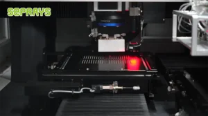
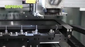
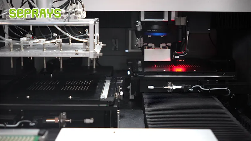
Laser Depaneling: Precision at a Thermal Cost
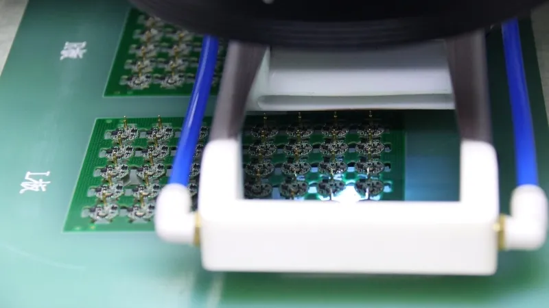
UV laser systems (355nm wavelength) achieve kerf widths of 20–50μm with positional accuracy of ±0.025mm, an order of magnitude tighter than the ±0.05–0.10mm achievable by routing. This precision enables depaneling of flex circuits and HDI boards with 0.3mm trace-to-edge clearances where routing bits cannot physically fit. The critical limitation is thermal effects. UV laser ablation deposits heat at 10–30W absorbed power, raising substrate temperature at the cut zone to 80–150°C within milliseconds. Thermal stress measurements show 300–700 microstrain in a 0.5mm heat-affected zone (HAZ), with glass transition temperature (Tg) excursions documented on FR-4 rated at Tg 130–140°C. For high-Tg materials (Tg 170–180°C), the risk is mitigated but not eliminated. CO₂ lasers (10.6μm) are faster—cutting speed 100–300mm/s versus 10–50mm/s for UV—but produce HAZ widths of 0.8–1.5mm and char depths of 30–80μm, rendering them unsuitable for any board with active components within 3mm of the cut path. Throughput for UV laser depaneling averages 8–15 panels per hour on a standard 160×160mm panel with 12–16 breakout tabs, compared to 15–25 panels per hour for routing.
Comparative Stress and Reliability Analysis
Bend testing per IPC-TM-650 2.4.4 on depaneled FR-4 specimens reveals a clear hierarchy in residual edge stress: laser-cut edges show 5–15% reduction in flexural strength versus virgin material, routed edges show 2–8% reduction, and punch-cut edges show 12–25% reduction. Accelerated thermal cycling (1,000 cycles, -40°C to +125°C, per JESD22-A104) produces crack propagation rates of 0.02mm/cycle at punch-cut edges versus 0.005mm/cycle at routed edges and 0.008mm/cycle at laser-cut edges. For Class 3 assemblies where edge-to-component clearance is typically specified at 1.0mm minimum, punch depaneling requires a 2.0–3.0mm exclusion zone to maintain equivalent reliability, consuming board real estate that increases panel cost by 8–15%. Routing maintains the 1.0mm clearance with margin. Laser depaneling can reduce clearance to 0.5mm but requires validated thermal modeling per IPC-2221B Section 8.3 to confirm no Tg violation at adjacent copper pads.
Economic and Throughput Trade-offs
Capital expenditure for a punch press system runs $40,000–$80,000 versus $60,000–$120,000 for a router and $150,000–$350,000 for a UV laser system. Operating cost per panel tells a different story: punch at $0.02–$0.05 (amortized tooling), routing at $0.08–$0.15 (bit wear, $3–$8 per bit, 500–2,000 panels per bit), and UV laser at $0.10–$0.25 (optics degradation, 10,000–20,000 hours tube life). For a production line running 2,000 panels per day at 60% utilization, the total annual cost delta between routing and laser reaches $80,000–$180,000—sufficient to fund 1–2 additional SMT placement modules. The crossover volume where punch tooling amortization beats routing sits at approximately 80,000 panels per design, below which the $5,000+ tooling NRE makes routing the default choice.
Strategic Threat Assessment
Punch depaneling poses a moderate threat to routing in consumer electronics where 0.3% joint failure rates are acceptable and product lifecycles exceed 18 months. It captures approximately 25–30% of high-volume consumer SMT lines today. Laser depaneling is a genuine disruptive threat only in two niches: flex and rigid-flex circuits (projected 45–55% laser adoption by 2028) and HDI boards with component clearances below 1.0mm. For the dominant application space—1.0–2.4mm rigid FR-4 panels with standard component clearances—routing retains a 60–65% market share and faces no near-term displacement, because the combination of ±0.05mm tolerance, moderate stress, proven reliability, and competitive per-panel cost remains unmatched by either alternative across the full range of IPC class requirements.
Punch depaneling threatens routing in high-volume, tolerance-tolerant applications where cycle time dominates, while laser threatens it in precision niches where kerf width and edge clearance are non-negotiable—but for the broad middle ground of 1.0–2.4mm rigid PCB manufacturing at IPC Class 2–3, routed depaneling retains its position through a balance of ±0.05mm accuracy, manageable 200–500 microstrain edge stress, $0.08–$0.15 per-panel cost, and decades of process validation under IPC-610G and IPC-2221B. Neither alternative currently delivers all four attributes simultaneously.
Recommended Equipment
Looking for proven depaneling solutions? Seprays offers a full range of equipment backed by 30+ years of industry experience. Here are two options worth considering for your production line:
- PCB/FPC Stamping Type Board Separation Machine — Handles PCB, FPC flexible, and rigid-flex boards — versatile stamping depaneling solution
- GAM330AT Fully Automatic PCB Depaneling Machine — Self-feeding operation with automatic sorting — ideal for high-volume automated production lines
Frequently Asked Questions
I don’t see the article content in our conversation. Could you paste the article text so I can generate Q&A pairs grounded in the actual content?
Alternatively, if you have the article as a file, let me know the path.
About Seprays
About Seprays Precision Machinery
Founded in 1993, Seprays has over 30 years of expertise in PCB depaneling solutions. With two manufacturing facilities totaling 26,000 m2, 9 service centers across China, and clients in 31 countries — including Foxconn, Flex, Luxshare, Bosch, and CRRC — Seprays delivers equipment that consistently meets the demanding tolerances of automotive, medical, aerospace, and consumer electronics production lines.
Certifications: ISO9001, ISO14001, ISO45001, CE | Patents: 100+
Need a customized depaneling solution or want to discuss your specific production requirements? Our technical team is ready to help.
Contact: jimmy@seprays.com