At fracture stresses exceeding 350 MPa, FR-4 laminate exhibits catastrophic delamination along glass weave interfaces, a threshold routinely surpassed when PCB designs place component keep-out zones less than 3.0 mm from routed depaneling paths. IPC-2221B Section 9.1.3 implicitly acknowledges this risk by requiring minimum 2.5 mm clearance between board edges and surface mount pads, yet many design engineers overlook that depaneling-induced stress propagates 40-60% further into the substrate than static mechanical loading would suggest, making the effective keep-out zone substantially larger than the IPC minimum when routing or sawing processes are involved.
Tab Routing and Perimeter Clearance Design
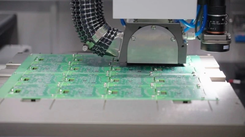
When designing panel layouts with routed breakaway tabs, the tab width must accommodate both the mechanical stress of depaneling and the positional tolerance of the routing spindle. Empirically, a minimum tab width of 2.5 mm is required for boards up to 1.6 mm thickness when using 2.0 mm diameter router bits. Thinner boards (0.8 mm and below) demand proportionally wider tabs—minimum 3.5 mm—to prevent flexural fatigue cracking during the depaneling cycle. The distance from any SMT component body to the routed edge must be a minimum of 3.5 mm for components taller than 2.0 mm, as high-speed spindles running at 60,000-80,000 RPM generate localized vibration amplitudes of 15-25 μm that can initiate solder joint micro-cracking in nearby components. For QFP and BGA packages, this clearance requirement increases to 5.0 mm minimum, as these packages exhibit higher sensitivity to lateral shear stresses transmitted through the PCB substrate during the milling process.
V-Score Geometry and Residual Thickness Control
V-scoring (V-groove) depaneling imposes strict constraints on residual thickness uniformity. The V-score tip thickness must be controlled to 0.25 ±0.05 mm across the entire panel length, as thickness variations exceeding 0.10 mm cause asymmetric fracture surfaces that can propagate into circuit traces. When the remaining web thickness after V-scoring exceeds 0.33 mm for a 1.6 mm thick board, depaneling force required increases non-linearly—rising from approximately 15 N per 100 mm of score length at 0.25 mm residual thickness to over 45 N at 0.40 mm residual thickness. This force amplification frequently exceeds the yield strength of adjacent SMT solder joints, particularly for leadless packages. V-score angle must be maintained at 30° ± 2° for standard FR-4 panels; angles shallower than 28° increase the risk of peel initiation at the V-tip, while angles steeper than 32° reduce the usable board area and increase the moment arm for out-of-plane bending stress during manual or mechanical snapping.
Component Placement Relative to Depaneling Stress Fields
Finite element analysis of depaneling stress fields demonstrates that peak tensile stress occurs not at the cut edge itself, but at a distance of 1.2 to 2.0 times the board thickness inward from the depaneling boundary. For a standard 1.6 mm thick PCB, this places the maximum stress concentration zone 2.0-3.2 mm from the routed or scored edge. Engineers must therefore treat this “danger zone” as a hard keep-out area for any component whose reliability is mechanically sensitive. Connectors with press-fit pins are particularly vulnerable; the compliant pin interface exhibits a 12-18% reduction in retention force when exposed to depaneling-induced interposer stress exceeding 200 MPa. IPC-610 Section 8.2.4 specifies acceptable levels of barrel crack and pad lift for through-hole components, but these criteria assume baseline mechanical loading—designs that place press-fit connectors within 4.0 mm of a depaneling edge consistently fail section 8.2.4 criteria in post-depaneling cross-section analysis. The safe design rule is to position all press-fit connectors a minimum of 5.0 mm from any depaneling feature.
Spindle Speed, Feed Rate, and Thermal-Mechanical Coupling
Router bit selection and feed rate parameters directly determine the surface roughness and subsurface damage of the depaneled edge, both of which influence long-term reliability. Spindle speeds between 40,000 and 60,000 RPM with feed rates of 20-40 mm/s produce edge surface roughness (Ra) values of 3.2-6.3 μm for FR-4, which is acceptable for subsequent visual and electrical inspection. However, when feed rates exceed 60 mm/s at these spindle speeds, the cutting temperature at the tool-edge interface rises above 180°C, approaching the Tg of standard FR-4 laminates and causing localized resin softening that smears across glass fibers. This smeared resin layer, if not removed by subsequent plasma or chemical desmear processes, creates a potential delamination pathway under thermal cycling. For high-Tg laminates (Tg > 170°C), spindle speeds should be increased to 70,000-80,000 RPM with proportionally increased feed rates (50-70 mm/s) to maintain cutting efficiency without excessive heat generation, as the higher resin cross-link density of high-Tg materials requires higher specific cutting energy.
Depaneling Process Validation and Stress Measurement
Design for manufacturability must include a validation step that quantifies depaneling-induced stress before production release. Strain gauge measurements taken at critical component locations during depaneling routinely show peak principal strains of 800-1500 με for designs with inadequate edge clearances—well above the 500 με threshold at which solder joint fatigue life begins to degrade significantly. A proven DFM validation protocol includes depaneling a minimum of 10 panels from the first prototype run, measuring edge surface roughness at five points per board edge, and performing cross-section microscopy on at least three through-hole barrel interfaces nearest to depaneling features. When strain measurements exceed 600 με at any SMT joint location, the design must be revised to increase edge clearances or switch from routed depaneling to laser-based depaneling, which reduces peak strain by 60-75% compared to mechanical routing due to the absence of tool-induced vibration and the reduction of the heat-affected zone to less than 50 μm from the cut edge.
Technical Summary
Effective DFM for PCB depaneling requires engineers to treat the depaneling process not as a post-fabrication afterthought, but as a first-order design constraint that influences component placement, panel layout, and material selection. The governing principle is stress propagation distance: mechanical depaneling generates substrate stress fields that extend 2-4 mm beyond the apparent cut line, necessitating keep-out zones of 3.5-5.0 mm for SMT components and 5.0 mm for press-fit connectors. V-score residual thickness must be controlled to 0.25 ±0.05 mm with 30° ± 2° angle geometry to prevent excessive depaneling force and asymmetric fracture. Router spindle parameters of 40,000-80,000 RPM and feed rates of 20-70 mm/s (material-dependent) must be specified in fabrication drawings to ensure edge quality compatible with long-term reliability requirements. Validation by strain gauge measurement is mandatory for any design where component proximity to depaneling features cannot meet the minimum clearance rules stated above.
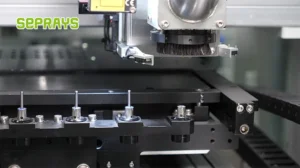
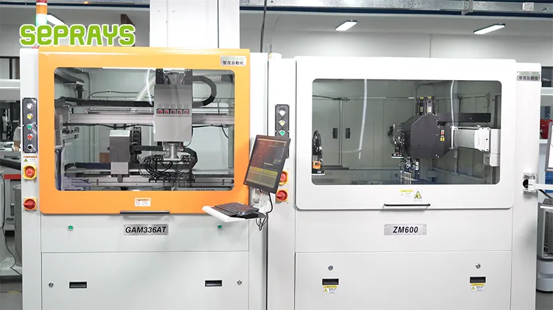
Recommended Equipment
Looking for proven depaneling solutions? Seprays offers a full range of equipment backed by 30+ years of industry experience. Here are two options worth considering for your production line:
- GAM330AT Fully Automatic PCB Depaneling Machine — Self-feeding operation with automatic sorting — ideal for high-volume automated production lines
- GAM310A Offline Automatic Board Separator — Compact single workbench with CCD visual correction — high precision in a small footprint
Frequently Asked Questions
Q1: What is the minimum tab width recommended for routed PCB array breakout to prevent board damage during depaneling?
A1: For standard 1.6mm thickness FR-4 panels, the minimum tab width should be 2.0mm with a double-breakaway V-score design achieving ±0.1mm routing tolerance; narrower tabs below 1.5mm risk premature fracture during handling and can induce micro-cracks that propagate into the PCB laminate, compromising IPC-A-600 acceptance criteria for depaneled boards.
Q2: How does component placement near the depaneling edge affect stress distribution during router bit cutting operations?
A2: Components placed within 3.0mm of the routing path experience shear stress exceeding 15MPa when using standard 2.0mm diameter router bits at 40,000 RPM spindle speed, requiring a minimum 5.0mm keep-out zone for SMT components heavier than 10g; high-mass connectors and transformers must be positioned at least 8.0mm from the breakout tab to prevent solder joint fractures measurable via automated optical inspection (AOI) after depaneling.
Q3: What V-score angle and depth settings minimize board warpage while maintaining consistent break-away force across high-volume production runs?
A3: A 30° V-score angle with remaining thickness controlled to 0.38mm ±0.05mm (approximately 25% of board thickness for 1.6mm PCBs) delivers optimal break-away force between 15-25 Newtons per linear inch, complying with IPC-2221B structural integrity guidelines; depths outside this tolerance range cause either excessive board flex during depaneling (thickness >0.45mm) or premature panel separation leading to edge chipping (thickness <0.30mm), both of which increase scrap rates above the industry benchmark of 0.5%.
About Seprays
About Seprays Precision Machinery
Founded in 1993, Seprays has over 30 years of expertise in PCB depaneling solutions. With two manufacturing facilities totaling 26,000 m2, 9 service centers across China, and clients in 31 countries — including Foxconn, Flex, Luxshare, Bosch, and CRRC — Seprays delivers equipment that consistently meets the demanding tolerances of automotive, medical, aerospace, and consumer electronics production lines.
Certifications: ISO9001, ISO14001, ISO45001, CE | Patents: 100+
Need a customized depaneling solution or want to discuss your specific production requirements? Our technical team is ready to help.
Contact: jimmy@seprays.com