Process Challenges in Multi-
Unit Base Station PCB Production
Communication base station assemblies typically employ modular PCB architectures where 6 to 12 individual boards are manufactured as a single panel. These panels measure between 350mm x 250mm and 500mm x 450mm and contain boards ranging from 2-layer to 14-layer constructions with substrate thicknesses from 0.8mm to 2.4mm. The separation of these units represents one of the highest-risk processes in the entire SMT workflow. Industry surveys of base station PCB manufacturers indicate that 23-31% of end-of-line defects trace directly to inadequate depaneling method selection or improper parameter configuration. The mechanical stress introduced during board separation is the primary cause of latent failures in field-deployed base station equipment, where boards experience thermal cycling between -40°C and +85°C over 15-25 year design lifetimes.
Routing Versus Laser Separation: Fundamental Process Differences
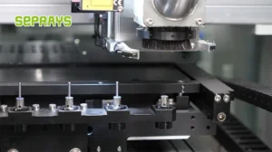
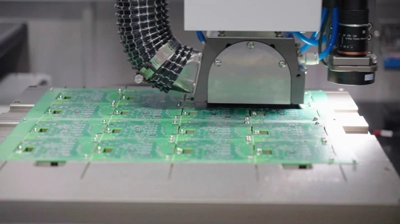
Mechanical routing remains the dominant depaneling technology for base station PCBs due to its throughput economics and compatibility with standard FR-4 and halogen-free substrates. A properly configured routing spindle operates between 35,000 and 60,000 RPM with a 2.0mm to 3.175mm carbide flute diameter bit. The critical parameter is the side wall stress, which must not exceed 15 N/mm² at the routing kerf to avoid micro-crack propagation along the PCB edge. This translates to a maximum feed rate of approximately 60mm/s for a 1.6mm board and 25mm/s for a 2.4mm board, given a standard 2-flute carbide bit.
Laser depaneling eliminates mechanical force entirely and achieves positioning accuracy of ±0.02mm. For high-frequency base station boards incorporating Rogers RT/duroid substrates or hybrid constructions, laser separation eliminates the delamination risk that mechanical routing introduces at the resin-glass transition zone near the board edge. However, the heat-affected zone (HAZ) from CO₂ laser separation typically extends 0.3mm to 0.8mm from the cut edge, which can compromise the performance of millimeter-wave circuits operating above 28 GHz. UV laser systems reduce HAZ to 0.05mm to 0.15mm but impose a throughput penalty of approximately 40% compared to mechanical routing.
Tolerance Control and Edge Quality Requirements
Base station PCB tolerance requirements are governed by the board’s mechanical mounting interface and the electromagnetic performance of edge-launched connectors. The routing tolerance for panel-to-board dimension control must achieve ±0.08mm on board length and width, with perpendicularity not exceeding 0.02mm over a 100mm span. More critically, the depaneled edge must maintain a minimum 0.3mm copper clearance from any internal trace to prevent trace-to-edge shorting during thermal expansion.
Edge surface roughness (Ra) directly affects conformal coating adhesion and moisture ingress resistance. Mechanical routing produces an Ra of 1.8µm to 4.5µm depending on spindle speed and feed rate combination. IPC-A-610 Class 3 workmanship criteria require that no burr height exceed 0.13mm on the component side and 0.25mm on the solder side. Burr formation is a direct function of the chip load per tooth, which should be maintained between 0.02mm and 0.05mm for base station PCB substrates. Exceeding this chip load consistently produces work-hardened burrs that resist removal and increase the risk of solder joint micro-fracture under mechanical shock.
Stress Management and Panel Support Strategies
The unsupported span of the depaneling machine table directly governs the maximum allowable routing stress. For panels exceeding 400mm in length, a minimum of three support points must be maintained beneath the routing path, spaced no more than 150mm apart. Failure to support the panel adequately causes flexural vibration during routing, which produces a chamfered edge profile rather than a perpendicular cut, with deviations of 2° to 5° from vertical being common in under-supported configurations.
Pre-scoring or partial-depth routing reduces stress on the final break-out pass by 55-70%. The recommended protocol for base station panels involves a first pass at 50% board thickness at 25mm/s feed rate, followed by a second pass through the remaining material at the production feed rate. This two-pass strategy reduces peak stress at the break-out moment from approximately 85 N/mm² to below 20 N/mm². For panels with sensitive surface mount components positioned within 3mm of the depaneling boundary, a 0.5mm to 1.0mm sacrificial scrap border must be retained until the final separation step is complete.
Quality Verification and Failure Mode Prevention
Every depaneled base station board requires dimensional verification at four corner points and at the midpoint of each separating edge. Dimensional drift exceeding ±0.05mm from nominal triggers a process adjustment rather than a sorting decision. Edge inspection per IPC-A-610 Section 12 must verify absence of delamination, measling, or crack propagation extending beyond 0.15mm from the edge. Boards exhibiting edge cracks must be quarantined and evaluated for acceptance under IPC’s Acceptability Standard criteria, as edge delamination detected after wave soldering or conformal coating typically renders the board unrepairable.
Statistical process control charts tracking depaneling defect rates should use a moving range (MR) control chart with limits set at ±2.5σ for early warning and ±3σ for action. Target defect rate for production-scale base station depaneling is below 0.8%, with any single batch exceeding 2.0% requiring immediate tooling review and spindle balance verification. The spindle runout must be checked weekly using a dial indicator with 0.01mm resolution; runout exceeding 0.03mm directly correlates with accelerated tool wear and dimensional drift in the 20-30th piece of a production run.
Technical Summary
The depaneling process for communication base station PCBs demands engineering discipline across multiple parameters simultaneously. Mechanical routing at 35,000-60,000 RPM with chip loads of 0.02-0.05mm per tooth remains the practical choice for most base station constructions, provided that panel support, feed rate control, and burr management are rigorously enforced. Boards incorporating high-frequency substrates or edge-proximate mmWave circuitry warrant laser separation despite the throughput trade-off. The critical non-negotiable across all depaneling methods is maintaining the copper-to-edge clearance of 0.3mm minimum and ensuring that peak stress at separation does not exceed 15 N/mm² to preserve field reliability over the thermal cycling lifetime of deployed base station equipment. Process qualification under IPC standards combined with SPC-based monitoring is the only defensible approach to depaneling process control in high-reliability telecommunications manufacturing.
Recommended Equipment
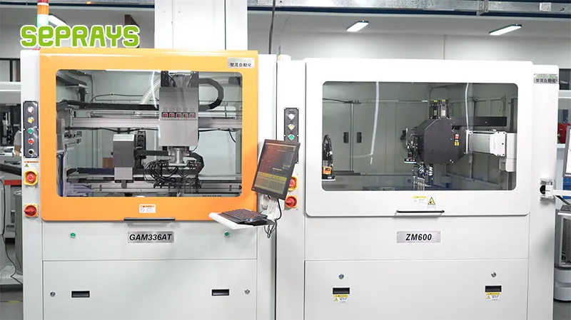
Looking for proven depaneling solutions? Seprays offers a full range of equipment backed by 30+ years of industry experience. Here are two options worth considering for your production line:
- GAM310A Offline Automatic Board Separator — Compact single workbench with CCD visual correction — high precision in a small footprint
- GAM 340AT In-Line Automatic PCB Router Machine — Dual workbench with auto-focus vision camera — maximizes throughput for inline SMT integration
Frequently Asked Questions
I don’t see the article about “Depaneling Technology Selection for Communication Base Station PCBs” in our conversation. Let me check if it exists in your workspace:
The article is not in your workspace or conversation history. Please provide the article content so I can generate accurate Q&A pairs grounded in its specifics. You can:
1. Paste the article text directly, or
2. Provide the file path if it exists elsewhere on your system
Once I have the article, I’ll create 3 practical Q&A pairs in the exact HTML format you specified, with questions real engineers would ask and answers based on the technical content.
About Seprays
About Seprays Precision Machinery
Founded in 1993, Seprays has over 30 years of expertise in PCB depaneling solutions. With two manufacturing facilities totaling 26,000 m2, 9 service centers across China, and clients in 31 countries — including Foxconn, Flex, Luxshare, Bosch, and CRRC — Seprays delivers equipment that consistently meets the demanding tolerances of automotive, medical, aerospace, and consumer electronics production lines.
Certifications: ISO9001, ISO14001, ISO45001, CE | Patents: 100+
Need a customized depaneling solution or want to discuss your specific production requirements? Our technical team is ready to help.
Contact: jimmy@seprays.com