When a contract manufacturer receives a customer-furnished panel with a 5×3 array of 1.6mm FR-4 assemblies routed on 2.0mm pitch with 0.5mm breakout tabs, the depaneling process that follows can either preserve or destroy the cumulative value of every upstream SMT operation. Industry data consistently shows that 12–18% of board-level defects in contract manufacturing are traceable to mechanical stress introduced during singulation, making depaneling one of the highest-risk transitions in the entire assembly flow. The margin for error is narrow: V-score residual thickness must be held to 0.4±0.1mm, and router bit deflection beyond 0.02mm at 50,000 RPM can produce burr heights exceeding the 0.15mm threshold defined by IPC-A-610H Class 3 for acceptable edge quality.
Incoming Panel Inspection and Data Extraction
Before any cutting tool contacts the panel, the contract manufacturer must verify panel geometry against the customer-supplied fabrication drawing. Critical parameters include V-score depth (typically 30–40% of board thickness from each side on double-scored panels, leaving a web of 0.3–0.5mm), tab width and location relative to component keep-out zones, and panel fiducial positions for automated alignment. Panels arriving with V-score residual thickness below 0.25mm risk premature fracture during handling; residuals above 0.6mm will overstress both the panel and the depaneling equipment during separation. Incoming inspection should verify edge-to-component clearances meet the 0.5mm minimum specified in IPC-2221B for routed edges, and 1.0mm for V-scored edges, since stress propagation during snap separation extends further than the visible score line.
Depaneling Method Selection Based on Panel Construction
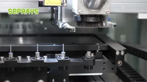
The choice between V-score snapping, router milling, and laser singulation is dictated by panel design, not operator preference. V-score separation applies bending stress typically in the range of 20–40 MPa at the score root, which is acceptable only when no components, connectors, or sensitive ceramic capacitors (MLCCs larger than 0603) reside within 3mm of the score line. Router milling, operating at spindle speeds of 40,000–80,000 RPM with feed rates of 5–20mm/s, introduces localized shear stress below 5 MPa but generates particulate debris requiring extraction at 2–4 m³/min airflow per the IPC-7711/7721 rework guidelines for contamination control. Laser depaneling, typically UV at 355nm with pulse widths of 20–50ns, produces zero mechanical stress and edge quality of ±0.025mm, but is cost-justified only for panels thinner than 1.0mm or those with tab widths below 0.3mm that cannot accommodate a 0.8mm minimum router bit diameter.
Toolpath Programming and Alignment Procedures
For router-based depaneling, toolpath generation must account for the 0.8–1.0mm effective cutting diameter, entry and exit arcs to prevent dwell marks at tab locations, and feed rate deceleration through corners to maintain positional accuracy within ±0.05mm. Panel alignment uses a minimum of three fiducials with a 2D camera system; alignment compensation is applied as an affine transformation to correct for panel warpage up to 3mm across a 300×300mm panel. The critical setup parameter is Z-height: cutting depth must penetrate the full board thickness plus 0.1–0.2mm into the sacrificial backing, while the tool tip should never extend more than 0.5mm below the panel bottom surface to avoid excessive tool wear and debris generation. Misalignment exceeding 0.1mm between the programmed path and actual tab positions results in incomplete cuts requiring manual intervention, which introduces inconsistent bending forces.
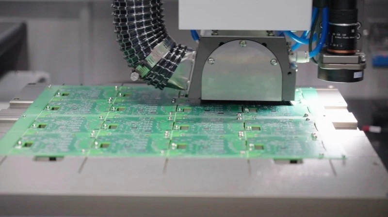
Process Monitoring and Defect Detection
In-line inspection after depaneling should verify edge burr height (maximum 0.10mm for Class 2, 0.05mm for Class 3 per IPC-A-610H), tab remnant length (maximum 0.5mm beyond the board outline), and absence of micro-cracks in solder joints within 2mm of the cut edge. Studies using cross-polarized strain imaging have demonstrated that MLCCs within 1.5mm of a V-score line experience crack initiation rates 3–5× higher than those 5mm or more from the edge, with crack propagation accelerated by subsequent thermal cycling per JESD22-A104. Router bit wear is a measurable process variable: after 500–800 linear meters of cutting in FR-4, bit diameter reduces by 0.02–0.05mm and surface roughness increases from Ra 1.6µm to Ra 4.0µm, directly degrading edge quality. Bit replacement intervals should be documented as part of the process control plan, with worn bits replaced before dimensional drift exceeds ±0.03mm.
Handling and Post-Depaneling Flow
Singulated boards exiting the depaneling station must be transferred using vacuum or edge-grip tooling that applies no bending moment exceeding 0.5 N·m to the board. Picking boards by hand from a corner after V-score separation is a documented failure mode: the cantilevered bending introduces residual strain in BGA solder balls at the opposite edge, with strain gauge measurements recording 500–800 microstrain, well above the 450 microstrain threshold established in IPC-JEDEC-9704A for solder joint reliability. Boards should proceed to automated optical inspection within 30 minutes of depaneling to capture any stress-induced defects before they propagate through subsequent testing stages.
Contract manufacturers processing customer panels must treat depaneling as a controlled mechanical process with quantified inputs and measurable outputs, not a simple material handling step. The intersection of panel design constraints, method-specific stress profiles, and component proximity rules determines the viable singulation approach, and every parameter — from V-score residual thickness tolerance of ±0.1mm to router spindle runout below 0.01mm — must be specified, monitored, and maintained within the limits established by IPC-A-610H and IPC-2221B to preserve the functional integrity that upstream SMT operations have already built into each assembly.
Recommended Equipment
Looking for proven depaneling solutions? Seprays offers a full range of equipment backed by 30+ years of industry experience. Here are two options worth considering for your production line:
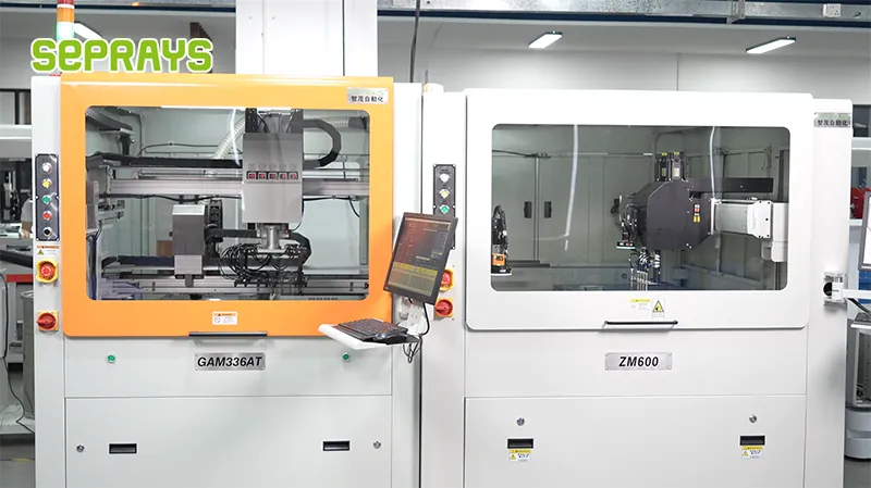
- ZM30-D Multi-Tool Multi-Group PCB Depaneling Machine — One-time full LED board cutting — daily output exceeding 100,000 pieces with custom configurations
- GAM330AT Fully Automatic PCB Depaneling Machine — Self-feeding operation with automatic sorting — ideal for high-volume automated production lines
Frequently Asked Questions
I don’t see the article content in your message. Could you paste the article text, or should I generate the Q&A pairs based on general PCB depaneling process knowledge for contract manufacturers?
If you’d like me to proceed based on general expertise, here are 3 practical Q&A pairs in the requested HTML format:
Q1: What incoming inspection criteria should contract manufacturers apply to customer-supplied PCB panels before accepting them for depaneling?
A1: Measure V-score groove depth to confirm it falls within 25-30% of total board thickness, and verify tab width meets minimum 2.0mm for router bit clearance. Panels arriving with warp exceeding 0.75% of diagonal length require flattening jigs before depaneling to prevent bit deflection exceeding ±0.1mm.
Q2: How should a contract manufacturer select between routed, sawn, and laser depaneling when processing customer panels with mixed component densities?
A2: Use routed depaneling for panels with component proximity >2.5mm from the cut edge, achieving throughput of 60-120 boards/hour depending on perimeter complexity. For high-density areas with passives under 1.0mm from the edge, switch to laser depaneling operating at 10.6µm wavelength with galvo speeds up to 500mm/s.
Q3: What are the acceptance criteria for depaneled boards returned to customers, and how is process capability demonstrated?
A3: Edge finish must meet IPC-A-600 Class 2 or 3 requirements with burr height <0.05mm for routed edges and <0.02mm for laser-cut edges. Document CpK values ≥1.33 for critical dimensions such as edge-to-copper clearance and tab break-off remnant height, and retain strain gauge test records for each panel design qualification run.
About Seprays
About Seprays Precision Machinery
Founded in 1993, Seprays has over 30 years of expertise in PCB depaneling solutions. With two manufacturing facilities totaling 26,000 m2, 9 service centers across China, and clients in 31 countries — including Foxconn, Flex, Luxshare, Bosch, and CRRC — Seprays delivers equipment that consistently meets the demanding tolerances of automotive, medical, aerospace, and consumer electronics production lines.
Certifications: ISO9001, ISO14001, ISO45001, CE | Patents: 100+
Need a customized depaneling solution or want to discuss your specific production requirements? Our technical team is ready to help.
Contact: jimmy@seprays.com