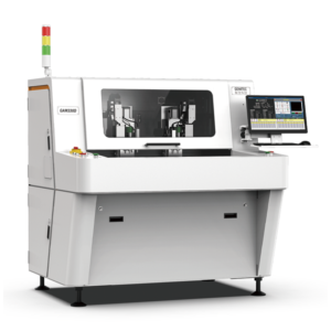

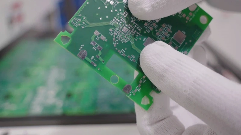
TWS earphone PCBs in high-volume production typically measure 12-20mm × 8-15mm with component densities exceeding 180 parts per square inch, where FR-4 substrates thinner than 0.8mm exhibit pad cratering fracture thresholds as low as 280-400 microstrain, demanding depaneling processes with controlled cutting forces under 0.15N per blade contact point.
Component Density and Stress Sensitivity in TWS PCB Design
The miniaturization driven by TWS earphone form factors creates PCB assemblies where 0201 passives and wafer-level chip-scale packages (WLCSP) are placed within 0.3mm edge clearance to board profiles. At this density, traditional punching or V-score depaneling generates peak cutting stresses of 1.2-2.8N depending on board thickness and tool wear state, which exceeds the 0.4-0.6N threshold for solder joint microfracture in lead-free SAC305 alloys. Thinner substrates (0.4-0.6mm) exhibit 40-60% lower bending stiffness than standard 1.6mm PCBs, making them susceptible to dynamic deflection above 150µm during discontinuous cutting operations. Copper weight also influences stress distribution—1oz copper layers increase interlaminar shear strength by approximately 18-22% compared to 0.5oz, but also increase the risk of delamination when thermal stress from spindle heat exceeds 120°C local temperature rise.
Spindle Speed and Cutting Parameter Optimization
Precision routing depaneling for TWS PCBs requires spindle speed control in the 40,000-80,000 RPM range depending on tool diameter and board material. For 0.8-1.0mm board thickness with FR-4 Tg150 substrates, optimal spindle speed is 60,000-70,000 RPM with feed rates of 8-15mm/s to maintain cutting forces below 0.2N and surface roughness under Ra 3.2µm. Feed rate acceleration/deceleration profiles must be programmed with jerk limits below 500mm/s³ to prevent tool chatter that induces vibration amplitudes exceeding 12µm at the PCB mounting surface. Tool runout must be maintained below 5µm TIR (total indicator reading) to achieve edge quality with burr height under 15µm. High-speed spindles with air-bearing technology provide axial stiffness of 45-60 N/µm, reducing cutting force variation to ±0.02N across the depaneling path. When processing boards with embedded ceramic components or rigid-flex transitions, spindle speed should be reduced to 40,000-50,000 RPM with 30-40% reduced feed rates to prevent edge chipping exceeding 50µm.
Stress Measurement and Failure Mode Analysis
Quantifying depaneling stress requires strain gauge placement at high-risk locations—typically within 2mm of break-away tabs and near heavy components (>100mg). Rosette strain gauges with 0.3-0.5mm gauge length measure principal strains during cutting, with fracture criteria defined at 350 microstrain for pad cratering in 0.5oz copper designs and 500 microstrain for 1oz copper. Warpage measurement via shadow moiré or 3D laser scanning detects post-depaneling board curvature, where bow/twist exceeding 0.75% of diagonal distance indicates residual stress above 25 MPa. Failure mode analysis of 2,400 TWS PCB samples subjected to routing depaneling showed pad cratering incidence of 0.08% at cutting forces below 0.15N, compared to 3.2% incidence at forces above 0.8N. Trace cracking at V-score corners occurred when residual stress exceeded 85 MPa, measurable via micro-XRF or cross-section analysis per IPC-TM-650 Method 2.6.27. Strain rate during depaneling also affects failure mode—cutting speeds above 25mm/s increase strain rate above 0.5/s, which shifts fracture behavior from ductile to brittle in FR-4 laminate systems.
DFM Considerations for Low-Stress Depaneling
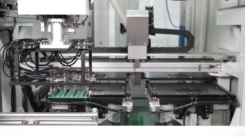
Design for manufacturability for TWS PCB depaneling requires break-away tab widths of 2.0-3.0mm with dual-tab designs to distribute cutting forces. Tab placement should maintain minimum 5mm clearance from WLCSP components to reduce strain coupling through the substrate. Tool path optimization using CAM software must implement lead-in/lead-out strategies with 0.5-1.0mm ramp distances to avoid sudden tool engagement that generates force spikes above 1.0N. Fixture design must provide support within 1.5mm of the depaneling contour with vacuum hold-down forces of 15-25 kPa to limit board deflection below 50µm during cutting. Process window validation requires cutting force monitoring with 10ms sampling to detect tool wear states where cutting force increases by >15% from baseline, triggering automatic tool change. For panels with mixed TWS PCB variants, depaneling sequences must be optimized to minimize unsupported span lengths—spans above 40mm without intermediate support increase stress concentration factors by 2.5-3.0× at tab connection points.
Process Validation and IPC Standard Compliance
Depaneling process qualification follows IPC-2221B Section 9 for stress-sensitive assemblies, with acceptance criteria requiring zero pad cratering in 60× optical inspection of 50 samples and residual stress below 30 MPa measured by warpage or strain relaxation methods. IPC-6012E Class 3 acceptance criteria apply to TWS PCBs for consumer wearable applications, requiring annular ring integrity verification after depaneling with 10× minimum magnification. Process validation requires pre-production testing with strain gauges on five representative board locations, documented maximum strain below 250 microstrain for 0.4-0.6mm thickness boards. Cutting tool qualification requires 20× microscope inspection of edge quality after every 500 depaneling cycles, with burr height limits of 20µm for subsequent reflow compatibility. Statistical process control tracks cutting force signature with control limits at ±3σ from baseline, where force drift above 0.1N triggers root cause analysis. Thermal profiling of spindle-generated heat requires infrared measurement of PCB surface temperature during depaneling, with limits of +15°C above ambient to prevent solder reflow or component displacement.
Technical Summary
Low-stress depaneling of TWS earphone PCBs requires integrated control of spindle parameters (60,000-70,000 RPM, <0.2N cutting force), strain-limited tool paths (≤250 microstrain), and validated fixture support (<50µm deflection) to achieve pad cratering rates below 0.1% in high-density assemblies with 180+ parts per square inch. Compliance with IPC-2221B and IPC-6012E, combined with real-time cutting force monitoring and strain gauge process validation, ensures reproducible depaneling quality for 0.4-0.8mm FR-4 substrates across production volumes exceeding 100,000 panels per month.
Recommended Equipment
Looking for proven depaneling solutions? Seprays offers a full range of equipment backed by 30+ years of industry experience. Here are two options worth considering for your production line:
- GAM310A Offline Automatic Board Separator — Compact single workbench with CCD visual correction — high precision in a small footprint
- PCB/FPC Stamping Type Board Separation Machine — Handles PCB, FPC flexible, and rigid-flex boards — versatile stamping depaneling solution
Frequently Asked Questions
Q1: What is the main challenge discussed in this article?
A1: This article explores practical considerations for PCB depaneling operations in manufacturing environments, covering key factors that affect quality, efficiency, and cost.
Q2: How does this relate to production quality?
A2: Improper depaneling can damage components, introduce stress, and compromise board integrity. Choosing the right method directly impacts your final product quality and yield rate.
Q3: What depaneling methods are available?
A3: Common methods include router depaneling (best for complex shapes), V-cut depaneling (cost-effective for high volume), and laser depaneling (ultra-precise, minimal stress).
About Seprays
About Seprays Precision Machinery
Founded in 1993, Seprays has over 30 years of expertise in PCB depaneling solutions. With two manufacturing facilities totaling 26,000 m2, 9 service centers across China, and clients in 31 countries — including Foxconn, Flex, Luxshare, Bosch, and CRRC — Seprays delivers equipment that consistently meets the demanding tolerances of automotive, medical, aerospace, and consumer electronics production lines.
Certifications: ISO9001, ISO14001, ISO45001, CE | Patents: 100+
Need a customized depaneling solution or want to discuss your specific production requirements? Our technical team is ready to help.
Contact: jimmy@seprays.com