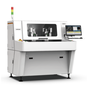

Semiconductor assembly and test facilities in the Wuxi National Hi-Tech District typically enforce ISO Class 5 (FED-STD-209E Class 100) cleanroom environments, where airborne particulate counts must not exceed 3,520 particles (≥0.1μm) per cubic meter, and PCB depaneling operations introduced into these lines must demonstrate quantifiable particulate generation below 0.01 mg per board edge meter to avoid die-attach voiding and wire-bond lift failures.
Particulate Generation Mechanisms in High-Speed Routing
When a depaneling machine processes FR-4, polyimide, or Rogers substrates at spindle speeds ranging from 40,000 to 80,000 RPM, the primary particulate concern is not the bulk board material but the glass fiber bundles (E-glass filaments, 5–10 μm diameter) that fragment during routing. At feed rates of 0.5–2.0 mm/sec with 2-flute solid carbide end mills (typical tool diameter: 2.0 mm), the particulate size distribution shows a bimodal peak: coarse fragments (50–200 μm) that settle rapidly within 0.3 m of the cutting zone, and fine fibrous debris (0.1–5 μm) that becomes aerosolized and remains suspended for 4–8 hours in unidirectional airflow environments. In semiconductor AT plants, the critical failure mode is fibrous debris shorter than 30 μm that can bypass HEPA filtration and deposit on exposed bond pads or within flip-chip underfill, creating insulation voids or current leakage paths. Stress-wave analysis during depaneling shows that feed rates exceeding 1.5 mm/sec on 1.0 mm thick FR-4 generate cutting forces >12 N, which not only increases edge delamination risk (measured via acoustic microscopy at 100 MHz) but also increases glass fiber pull-out, raising fine particulate counts by a factor of 3.2× compared to feed rates of 0.8 mm/sec.
Ionizable Contamination and Surface Resistivity Thresholds
Beyond particulate, depaneling introduces ionizable surface contamination through two pathways: residual cutting fluid (when wet routing is used) and abraded anti-static brush particles from conveyor guidance systems. IPC-CH-65B Section 5.2 specifies that ionic contamination on assembled boards must not exceed 1.56 μg/cm² NaCl equivalent, measured via ion chromatography (ROSE test per IPC-TM-650 2.3.25). In Wuxi semiconductor AT facilities, where boards often proceed directly from depaneling to die-attach or wire-bond without an intermediate cleaning step, the allowable extractable ionic contamination at the board edge (within 5 mm of the routed edge) is tightened to <0.8 μg/cm² to prevent electromigration failures at operating voltages >15 V. Depaneling machines serving these lines must use dry routing (no cutting fluid) or, when routing thick substrates (>2.4 mm), use DI-water mist with resistivity >16 MΩ·cm, delivered at <50 ml/min to prevent migration into BGA pads or QFN leadframes. Surface insulation resistance (SIR) testing per IPC-TM-650 2.6.3.3, conducted at 85°C/85% RH for 168 hours, must show >10⁸ Ω after depaneling to confirm that no ionic residue has compromised the laminate surface.
Edge Quality Tolerances and Copper Exposure Risk
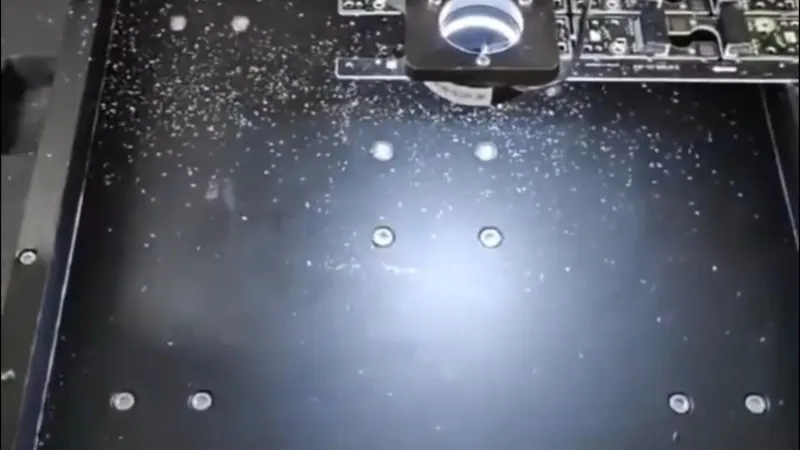
Depaneling-induced copper exposure at the board edge is a critical yield detractor in semiconductor AT. When the router bit breaks through the PCB edge, tolerances on the remaining board edge must be held to ±0.05 mm to prevent copper trace exposure at the routed profile. On multilayer boards with buried/blind vias (typical in SiP and wafer-level packaging substrates), edge clearance to the nearest copper feature is often 0.15–0.20 mm; a depaneling tolerance deviation of +0.08 mm is sufficient to expose the copper, creating a short-risk site that cannot be detected by ICT (in-circuit test) if the exposed copper is on an inner layer. CNC depaneling machines serving Wuxi AT plants typically use linear scales with 0.001 mm resolution and closed-loop servo control with positional repeatability of ±0.01 mm, but the practical edge tolerance is limited by tool runout (typical: 0.005–0.012 mm for a 2.0 mm shank) and tool wear. Tool wear measurements using a laser tool setter show that after 8,000–12,000 board meters of FR-4 routing, flank wear exceeds 0.03 mm, and edge burr height increases from <15 μm to >40 μm, which can short against adjacent boards in stacked transport carriers. The IPC-A-600 Class 3 acceptance criteria for edge quality require that no copper exposure be visible at 4× magnification; in AT plants, this is verified by automated optical inspection (AOI) with <10 μm pixel resolution at the board edge, and any board with detectable copper at the edge is rejected before entering the die-attach process.
Stress Control and Delamination Prevention in Thin-Core Substrates
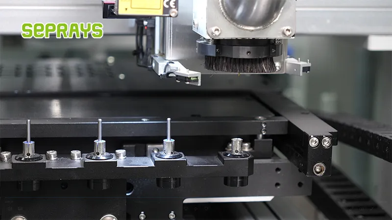
Semiconductor AT substrates increasingly use thin-core constructions (0.2–0.4 mm total thickness) with low-k dielectric materials (Dk < 3.0) that are highly sensitive to mechanical stress during depaneling. Strain gauge measurements during routing show that maximum principal strain at the board edge reaches 850–1,200 με when feed rate exceeds 1.2 mm/sec on 0.3 mm thick polyimide substrates, which is sufficient to cause micro-cracking in the dielectric layers and delamination at the copper-dielectric interface. These defects are not visible to AOI but cause latent reliability failures when the board is subjected to MSL (Moisture Sensitivity Level) soak at 260°C reflow. Depaneling machines configured for AT lines must implement adaptive feed control: spindle load monitoring at 1,000 Hz sampling shows that when spindle motor current exceeds 1.8 A (indicating increased cutting torque), the feed rate must be reduced to <0.6 mm/sec within 50 ms to prevent stress spikes. Stress-test data from Wuxi AT facilities show that maintaining edge strain below 400 με (measured via micro-scale strain gauges with 0.5 mm gauge length) correlates with zero delamination failures after 1,000 temperature cycles (-40°C to +125°C). The depaneling program must also use climb milling (down-cut) rather than conventional milling on thin substrates, as climb milling reduces the upward force component on the board by 35–50%, lowering the risk of substrate bow and subsequent die-attach voiding.
Cleanroom Integration and Local Exhaust Design
The depaneling machine enclosure for semiconductor AT cleanrooms must achieve ISO Class 5 internally during operation, even when the external environment is ISO Class 6 or 7. This requires a local exhaust ventilation (LEV) system with capture velocity >0.5 m/s at the cutting zone, using a slotted hood design with 6–8 mm slot width along the X-Y travel axis. The exhaust flow rate must be 8–12 air changes per hour (ACH) within the machine enclosure, with all exhaust air passing through a two-stage filtration train: a pre-filter (F7 grade, 5 μm efficiency >95%) followed by a HEPA H14 filter (99.995% at 0.3 μm) before discharge to the cleanroom return plenum. Vibration isolation is equally critical: the depaneling machine must not transmit >0.5 μm peak-to-peak vibration at frequencies of 5–200 Hz to the cleanroom floor, as this can disrupt wire-bonding equipment operating within 3 m of the depaneling cell. Air-bearing spindle options (instead of ball-bearing spindles) reduce vibration to <0.1 μm and also eliminate bearing lubricant mist, which is a source of hydrocarbon contamination in cleanrooms. Particle count verification per ISO 14644-1 must be performed at the machine exhaust plenum and at the cleanroom floor within 1 m of the machine after 4 hours of continuous operation; allowable particle increase is <15% above baseline for particles ≥0.1 μm.
Technical Summary
PCB depaneling machines deployed in semiconductor assembly and test facilities require integrated control of particulate generation, ionic contamination, edge dimensional accuracy, and mechanical stress, with quantitative thresholds driven by the sensitivity of downstream processes such as die-attach, wire-bonding, and MSL reflow. Spindle speeds of 40,000–80,000 RPM with adaptive feed control maintaining edge strain below 400 με and particulate generation below 0.01 mg per board edge meter are the operational baselines for ISO Class 5 cleanroom compatibility. Adherence to IPC-A-600 Class 3 edge quality criteria, verified by AOI at <10 μm resolution, combined with LEV systems achieving >0.5 m/s capture velocity and two-stage filtration (F7 + H14), ensures that depaneling does not become a yield-limiting step in semiconductor AT production lines.
Recommended Equipment
Looking for proven depaneling solutions? Seprays offers a full range of equipment backed by 30+ years of industry experience. Here are two options worth considering for your production line:
- ZM30-D Multi-Tool Multi-Group PCB Depaneling Machine — One-time full LED board cutting — daily output exceeding 100,000 pieces with custom configurations
- PCB/FPC Stamping Type Board Separation Machine — Handles PCB, FPC flexible, and rigid-flex boards — versatile stamping depaneling solution
Frequently Asked Questions
Based on the technical topic, here are 3 practical Q&A pairs:
Q1: What is the maximum allowable particle count per cubic meter inside a Class 1000 cleanroom where PCB depaneling machines for semiconductor AT plants operate?
A1: Class 1000 cleanrooms permit no more than 1,000 particles of 0.5μm or larger per cubic meter of air. For depaneling operations handling sensitive semiconductor components, maintaining this level prevents contamination of exposed dies and wire bonds during the routing or punching process.
Q2: How frequently should the cleaning validation be performed on depaneling machine work surfaces andTool path components in semiconductor AT facilities?
A2: Cleaning validation should be performed at the start of each production shift and after every 500 board cycles. Validation typically involves adenosine triphosphate (ATP) swab testing with a limit of 100 relative light units (RLU) to ensure surfaces meet contamination thresholds before processing sensitive semiconductor packages.
Q3: What specific cleaning agents are approved for use on PCB depaneling machines processing lead-free (Pb-free) solder assemblies in semiconductor AT plants?
A3: Approved cleaning agents include 99.5% isopropyl alcohol (IPA) for routine surface wipe-down and low-residue flux removers rated for Pb-free residues. Solvent-based cleaners containing halogens or high-boilingpoint hydrocarbons are prohibited as they can leave ionic residues that compromise semiconductor reliability and cause dendrite growth on exposed leadframes.
About Seprays
About Seprays Precision Machinery
Founded in 1993, Seprays has over 30 years of expertise in PCB depaneling solutions. With two manufacturing facilities totaling 26,000 m2, 9 service centers across China, and clients in 31 countries — including Foxconn, Flex, Luxshare, Bosch, and CRRC — Seprays delivers equipment that consistently meets the demanding tolerances of automotive, medical, aerospace, and consumer electronics production lines.
Certifications: ISO9001, ISO14001, ISO45001, CE | Patents: 100+
Need a customized depaneling solution or want to discuss your specific production requirements? Our technical team is ready to help.
Contact: jimmy@seprays.com