A typical 1.6mm FR-4 panel with 0.5mm breakout tabs can withstand approximately 120 N of tensile force before fracture — yet poorly executed depaneling routinely subjects those same tabs to localized stresses exceeding 300 MPa, cracking solder joints within 2 mm of the singulation edge and reducing first-pass yield by 8–15%. Depaneling — the process of separating individual printed circuit boards from a fabrication panel — is therefore not merely a mechanical cut, but a precision operation whose stress profile directly governs downstream reliability, especially for assemblies conforming to IPC-A-610 Class 3 requirements.
Singulation Methods and Their Mechanical Signatures
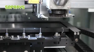
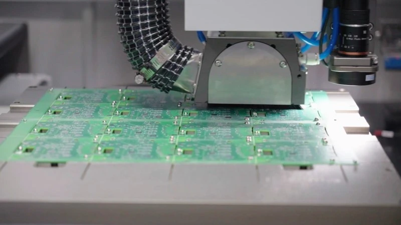
Five principal depaneling methods dominate volume production: manual breaking, V-score snapping, router milling, laser cutting, and punch die stamping. Each produces a distinct stress signature. Manual breaking of routed breakout tabs generates impulse loads of 200–400 N over durations shorter than 5 ms, sufficient to delaminate boards with copper weights above 2 oz or flex-rigid stackups. V-score snapping — where a pre-scored groove (typically 0.4–0.6 mm residual web on a 1.6 mm board) is fractured by a wedge fixture — applies controlled bending at 1–3 mm/s and keeps peak stress under 80 MPa, well below the 280 MPa flexural strength of standard FR-4. Router milling removes material at spindle speeds of 40,000–80,000 RPM with feed rates of 5–20 mm/s, producing negligible mechanical stress on adjacent components but introducing particulate contamination that requires class 10,000 extraction. UV laser cutting (355 nm) achieves kerf widths of 20–50 µm with positional accuracy of ±0.025 mm, while CO₂ laser systems (10.6 µm) reach ±0.05 mm but char the cut edge, producing a heat-affected zone of 50–200 µm that is unacceptable for high-frequency substrates. Punch die stamping, reserved for high-volume rigid boards, delivers singulation rates exceeding 1,000 panels per hour with positional repeatability of ±0.02 mm, but tooling cost and zero flexibility limit it to stable, long-run products.
Routing Parameters and Burr Control
Router-based depaneling remains the most versatile method for mixed-technology panels containing components mounted within 2 mm of the breakaway edge. Critical parameters include spindle runout (must be below 5 µm TIR to prevent chattering), chip load per tooth (0.005–0.015 mm for 1.6 mm FR-4 using a 2.0 mm diameter single-flute carbide bit), and cutting depth per pass. Single-pass cutting at full board thickness risks burr heights of 30–80 µm at the exit side; a two-pass strategy — roughing at 80% depth followed by a finish pass at full depth — reduces exit burrs to under 10 µm. Spindle speed must be maintained within ±2% of the programmed RPM: at 60,000 RPM on a 2-flute cutter, a 3% underspeed increases chip load by 3%, accelerating tool wear and raising burr height above the 25 µm threshold specified by IPC-A-610 Section 10.3 for acceptable edge finish. Tool life is typically 8,000–15,000 linear meters of cut in standard FR-4; halving that figure in high-Tg (Tg ≥ 170 °C) or ceramic-filled laminates is common.
Laser Depaneling: Precision and Thermal Constraints
UV laser depaneling operates at pulse durations of 10–30 ns and pulse repetition rates of 80–200 kHz, ablating material layer by layer with per-pulse removal depths of 5–15 µm. For a 1.6 mm board, this requires approximately 100–320 passes, yielding singulation times of 15–45 seconds per board depending on contour length. The critical metric is the heat-affected zone: UV systems at 355 nm keep thermal damage below 25 µm from the kerf, preserving dielectric properties within the ±0.02 Dk tolerance required for impedance-controlled traces per IPC-4101. Green laser systems (532 nm) occupy a middle ground, with HAZ of 30–80 µm and cutting speeds 2–3× faster than UV. Fiber laser depaneling (1064 nm) is unsuitable for standard FR-4 due to excessive charring but finds application on metal-core PCBs where the aluminum substrate requires higher power density. All laser systems require fume extraction rated at minimum 200 m³/h with HEPA and activated carbon stages to capture copper and glass particulate below 0.3 µm.
Stress-Sensitive Components and Proximity Rules
Depaneling-induced stress propagates through the board as a transient flexural wave. Components most vulnerable to this stress — BGA packages with 0.3 mm pitch, 0201 chip components, and ceramic capacitors larger than 0603 — must observe minimum keep-out distances from the singulation edge. IPC-2221B recommends a minimum edge distance of 2.5 mm for components on the primary side; however, empirical failure analysis data shows that for router-milled panels, 2.0 mm is sufficient, while for V-score snapped panels, 3.0 mm is required due to the higher bending moment. For boards thicker than 2.4 mm, the bending stiffness increases by a factor of approximately 3.4 relative to 1.6 mm (stiffness scales with the cube of thickness), allowing reduced keep-out distances. Strain gauge measurements on 1.0 mm thick assemblies routed at 50,000 RPM and 10 mm/s feed rate record peak strains of 150–250 µε at 2 mm from the cut — below the 500 µε threshold that triggers solder joint cracking per IPC-9702 strain gauge guidelines.
Process Selection Framework
Choosing the optimal depaneling method requires balancing four variables: panel complexity, component proximity, throughput requirement, and acceptable edge quality. For panels with components within 1.5 mm of the edge and impedance-controlled traces, UV laser cutting at ±0.025 mm accuracy is the only method that simultaneously satisfies zero mechanical stress and dielectric integrity requirements. For high-mix, medium-volume production where component density varies panel to panel, router milling with dual-pass strategy and automated tool wear compensation provides the best cost-per-cut at $0.02–0.08 per board. V-score snapping remains the lowest-cost option at under $0.01 per board for designs with keep-out zones of 3 mm or more and no flex sections. Punch stamping achieves the lowest per-unit cost below $0.005 at volumes above 500,000 units, provided tooling amortization justifies the $15,000–$40,000 die investment. Across all methods, in-line inspection of the singulated edge — whether by machine vision checking burr height against the 25 µm IPC threshold or by cross-section measurement of HAZ depth — is essential to closing the quality loop.
Depaneling is a precision mechanical and thermal process whose method selection, parameter control, and edge-quality verification directly determine solder joint reliability and board-level electrical performance; matching spindle speed tolerance, laser pulse energy, or snap fixture geometry to the specific panel stackup and component proximity constraints — within the quantitative limits defined by IPC-A-610, IPC-2221, and IPC-9702 — is what separates a 98% first-pass yield from a costly 85% rework loop.
Recommended Equipment
Looking for proven depaneling solutions? Seprays offers a full range of equipment backed by 30+ years of industry experience. Here are two options worth considering for your production line:
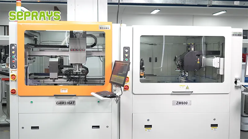
- GAM 340AT In-Line Automatic PCB Router Machine — Dual workbench with auto-focus vision camera — maximizes throughput for inline SMT integration
- PCB/FPC Stamping Type Board Separation Machine — Handles PCB, FPC flexible, and rigid-flex boards — versatile stamping depaneling solution
Frequently Asked Questions
Q1: What is the main challenge discussed in this article?
A1: This article explores practical considerations for PCB depaneling operations in manufacturing environments, covering key factors that affect quality, efficiency, and cost.
Q2: How does this relate to production quality?
A2: Improper depaneling can damage components, introduce stress, and compromise board integrity. Choosing the right method directly impacts your final product quality and yield rate.
Q3: What depaneling methods are available?
A3: Common methods include router depaneling (best for complex shapes), V-cut depaneling (cost-effective for high volume), and laser depaneling (ultra-precise, minimal stress).
About Seprays
About Seprays Precision Machinery
Founded in 1993, Seprays has over 30 years of expertise in PCB depaneling solutions. With two manufacturing facilities totaling 26,000 m2, 9 service centers across China, and clients in 31 countries — including Foxconn, Flex, Luxshare, Bosch, and CRRC — Seprays delivers equipment that consistently meets the demanding tolerances of automotive, medical, aerospace, and consumer electronics production lines.
Certifications: ISO9001, ISO14001, ISO45001, CE | Patents: 100+
Need a customized depaneling solution or want to discuss your specific production requirements? Our technical team is ready to help.
Contact: jimmy@seprays.com