A single 0.1mm routing deviation on a populated PCB can induce stress concentrations exceeding 15 N/mm² in adjacent component lead regions, triggering early failure modes in consumer electronics assemblies running at production volumes exceeding 50,000 units per day. This stark reality defines the central challenge facing manufacturing engineers: achieving throughput rates above 600 boards per hour while maintaining the ±0.05mm positional accuracy demanded by modern miniaturized circuit assemblies.
Mechanical Stress and Fracture Risk in Depaneling Operations
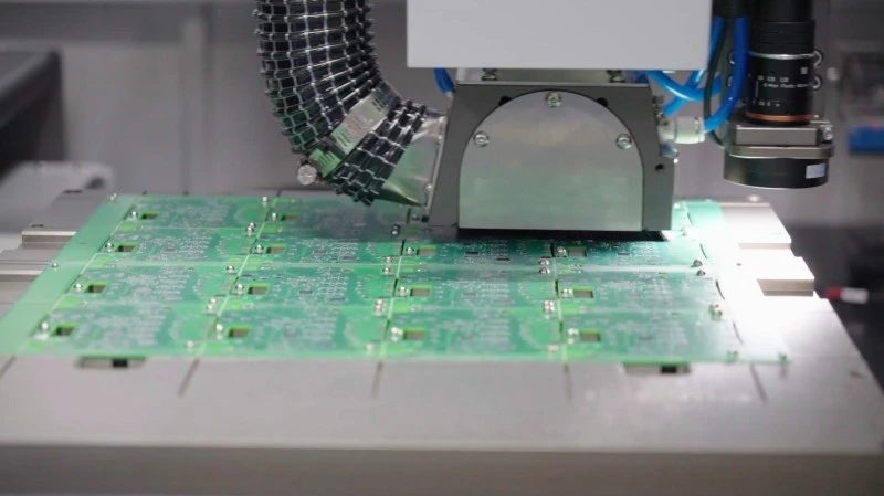
The depaneling process imposes significant mechanical loading on FR-4 and polyimide substrates, with routing operations generating intermittent cutting forces ranging from 0.5 to 3.2 N depending on bit geometry and feed rate. These transient loads propagate through the panel, concentrating at stress risers created by incomplete score lines or pre-arranged V-grooves. Research indicates that boards with component heights exceeding 15mm experience up to 40% higher defect rates when routed at feed rates above 300mm/min, as cantilever vibration amplifies fracture risk at the breakout point.
Finite element analysis of typical 1.6mm thick six-layer boards reveals that conventional router bits create a heat-affected zone extending 0.3-0.5mm from the cut edge, degrading dielectric properties in that boundary layer. This thermal gradient, combined with mechanical stress, initiates micro-crack propagation along glass fiber weave paths. Quality engineers must recognize that visual inspection alone misses approximately 35% of stress-induced delamination defects, necessitating acoustic microscopy or X-ray inspection for comprehensive quality assurance.
Feed Rate Optimization and Positional Accuracy Trade-offs
High-speed routing demands careful balance between spindle RPM and table feed rate, typically expressed as chip load per tooth. Operating spindle speeds of 40,000 to 60,000 RPM with 0.8-1.2mm diameter bits requires chip loads between 0.02 and 0.05mm per revolution to avoid excessive heat generation and bit wear. At these parameters, achievable feed rates range from 150 to 400mm/min depending on panel thickness and number of penetrations required.
Advanced interpolation algorithms enabling smooth acceleration/deceleration transitions reduce dynamic positioning error to below ±0.02mm during curved routing paths, but this precision comes at a throughput cost of approximately 15-20% reduction compared to aggressive linear cutting profiles. Manufacturers processing rigid-flex boards face additional complexity, as the flexible substrate sections require reduced feed rates of 80-120mm/min to prevent tearing at the routing exit point, effectively creating a bottleneck in otherwise high-speed production lines.
Tool Wear Dynamics and Process Consistency
Carbide router bits exhibit predictable wear patterns directly correlated with cumulative cutting distance and material hardness variations across panel batches. Empirical data shows that bit diameter decreases by 0.02-0.04mm after 200-300 linear meters of cutting in standard CEM-1/CEM-3 substrates, while ceramic and diamond-coated bits extend this interval to 800-1,200 linear meters. However, even minor bit wear amplifies cut edge roughness from Ra 1.6μm to Ra 3.2μm or higher, potentially violating IPC-A
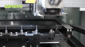
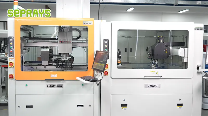
Recommended Equipment
Looking for proven depaneling solutions? Seprays offers a full range of equipment backed by 30+ years of industry experience. Here are two options worth considering for your production line:
- ZM30-D Multi-Tool Multi-Group PCB Depaneling Machine — One-time full LED board cutting — daily output exceeding 100,000 pieces with custom configurations
- GAM330AT Fully Automatic PCB Depaneling Machine — Self-feeding operation with automatic sorting — ideal for high-volume automated production lines
Frequently Asked Questions
Q1: What is the primary efficiency bottleneck in high-volume PCB depaneling operations for consumer electronics?
A1: The dominant bottleneck is the trade-off between cutting speed and component stress tolerance. High-speed routing generates vibration that can damage sensitive SMT components, particularly ceramic capacitors and BGA packages, forcing manufacturers to reduce throughput to maintain quality yields below 0.5% rejects.
Q2: How does tool wear impact depaneling consistency in round-the-clock production environments?
A2: Blade degradation causes increasing friction and heat buildup after approximately 2,000-3,000 cutting cycles, resulting in solder joint microcracks and board delamination. Without real-time monitoring systems, operators often detect wear only through quality failures, causing unplanned downtime that can reduce overall equipment effectiveness by 15-25%.
Q3: What depaneling method provides the best balance between speed and precision for mixed-size panel configurations?
A3: Laser depaneling eliminates mechanical stress entirely and handles complex geometries without tooling changes, but the lower throughput of 80-120 boards per hour compared to 400+ for routing makes it cost-prohibitive for commodity products. The optimal approach typically uses routing for standardized rectangles with laser finishing for stress-sensitive boards, per IPC-7721 guidelines.
About Seprays
About Seprays Precision Machinery
Founded in 1993, Seprays has over 30 years of expertise in PCB depaneling solutions. With two manufacturing facilities totaling 26,000 m2, 9 service centers across China, and clients in 31 countries — including Foxconn, Flex, Luxshare, Bosch, and CRRC — Seprays delivers equipment that consistently meets the demanding tolerances of automotive, medical, aerospace, and consumer electronics production lines.
Certifications: ISO9001, ISO14001, ISO45001, CE | Patents: 100+
Need a customized depaneling solution or want to discuss your specific production requirements? Our technical team is ready to help.
Contact: jimmy@seprays.com