How Laser Depaneling Improves PCB Quality
When a contract manufacturer in Southeast Asia transitioned 23 production lines from router-based depaneling to UV laser systems in 2023, the first-scan defect rate on complex multi-panel assemblies dropped from 847 ppm to 31 ppm within eight weeks. That single data point encapsulates why laser depaneling has become the preferred method for high-density PCB assemblies: it eliminates the root cause of mechanical-stress failures that plague every physical separation process.
Mechanical Stress in Traditional Depaneling Methods
All physical board separation techniques — V-scoring with snap separation, plunge routing, and sawing — share a common failure mechanism: they transfer lateral and torsional forces directly into the panel. Plunge routing applies a radial cutting force of 5–15 N at the bit tip while simultaneously imposing a bending moment that propagates through the panel thickness. On a 1.6 mm FR-4 board with 12-row BGA arrays, this combination routinely produces crack propagation along fillet boundaries within 72 hours of assembly. IPC-A-610H Section 12.1 defines the acceptability criteria for board integrity post-depanelization, and mechanical methods consistently fail the micro-crack detection criteria when inspected under 40× magnification with transmitted light.
The tool wear problem compounds the stress issue. Tungsten carbide routing bits begin degrading after approximately 1,200 linear meters of cut on standard CEM-1 substrates. As the cutting edge radius increases from the fresh 0.15 mm specification to 0.35–0.40 mm near end-of-life, the lateral force requirement rises by 40–60%, directly increasing the risk of laminate delamination at internal plane layers. Even with automated tool-life management systems, the statistical spread of cut quality widens significantly in the final 15% of a bit’s usable life.
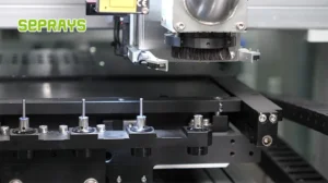
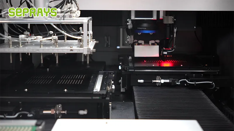
The Laser Alternative: Non-Contact Material Removal
UV laser depaneling at 355 nm wavelength operates through photomechanical ablation rather than thermal cutting. The ultra-short pulse duration — typically 10–20 picoseconds in modern systems — deposits energy into the dielectric material faster than thermal diffusion can occur, creating micro-explosions that eject material without raising the surrounding substrate temperature above 80°C. For comparison, standard FR-4 begins glass transition at approximately 130°C, meaning properly tuned UV laser systems operate well below the Tg threshold throughout the entire cutting process.
CO2 laser systems at 10.6 μm wavelength operate differently, targeting the organic resin matrix through purely thermal decomposition. These systems require careful power management because the heat-affected zone (HAZ) extends 50–150 μm beyond the kerf width depending on pulse frequency and assist gas configuration. UV laser systems, by contrast, confine the HAZ to within 10–25 μm of the cut edge, making them the preferred choice for boards with trace-to-edge distances below 0.3 mm.
Precision, Repeatability, and Geometric Flexibility
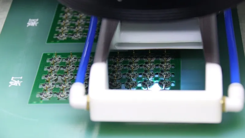
Laser systems achieve positioning accuracy of ±0.02 mm with repeatability of ±0.03 mm (2σ) when equipped with linear encoders and active motion control. This compares favorably against router spindles, which typically deliver ±0.08 mm accuracy and ±0.10 mm repeatability under production feed rates of 150–200 mm/s. The positional advantage becomes critical on panels with tight tolerances between routed slots and component pads — a 0.5 mm clearance between a shielded can and the board edge demands the tighter tolerance band that laser systems provide.
Geometric flexibility represents an equally important advantage. While routers require physical bit changes to alter cut profiles, laser systems reconfigure cut paths entirely through software without any mechanical changeover. This enables complex contoured cuts — rounded corners, stepped transitions, and multi-depth channel routing — that are impractical or impossible with end mills. For assemblies incorporating insert-molded housings or snap-fit features that require precise edge geometry, laser depaneling delivers the as-designed geometry without compromising feature dimensions.
Heat Management and Heat-Affected Zone Control
The HAZ concern in laser depaneling demands active management through parameter optimization. For standard 1.6 mm FR-4 panels, a properly tuned UV laser operating at 30 kHz pulse repetition rate and 2 W average power produces a kerf width of 40–60 μm with a thermal damage zone of less than 20 μm. Nitrogen assist gas at 0.4–0.6 MPa pressure expels debris and suppresses secondary thermal damage along the cut face. When these parameters are held within specification, copper traces located 0.2 mm from the cut edge show no measurable degradation in peel strength or conductivity after 1,000 thermal cycles between -40°C and +125°C per IPC-TM-650 Method 2.6.27.
Power scaling for thicker panels — 2.4 mm and 3.2 mm boards used in power electronics — requires proportional increases in pulse energy and reduction in traverse speed, typically maintaining a constant fluence of 0.8–1.2 J/cm² to preserve HAZ integrity regardless of total board thickness.
Contamination, Debris, and Cleanroom Compatibility
Mechanical depaneling generates particulate contamination proportional to cut volume: a 1-meter router slot in 1.6 mm FR-4 produces 4–7 grams of fibrous debris requiring extraction and filtration. In cleanroom environments rated to ISO Class 7 (10,000 particles per cubic meter at 0.5 μm), this debris load immediately exceeds acceptable thresholds unless aggressive extraction systems are operating at 95%+ capture efficiency. Laser depaneling produces no fibrous debris; the ablated material converts to vapor and fine particulate (<1 μm) that standard HEPA filtration handles efficiently. This makes laser systems inherently cleaner and more suitable for medical device and aerospace PCB assembly lines where contamination control is mandatory.
Technical Summary
Laser depaneling fundamentally improves PCB quality through three mechanisms: elimination of mechanical stress that causes micro-cracks and solder joint failures, sub-0.05 mm positional accuracy and repeatability that protects tight clearances between components and board edges, and minimal heat-affected zones that preserve laminate integrity and trace adhesion at the cut boundary. While the capital cost of laser systems exceeds that of router equipment by a factor of 2.5–4×, the reduction in defect-related rework costs, the elimination of consumable tool inventory, and the improvement in first-pass yield on high-value assemblies typically deliver full ROI within 14–22 months of production deployment. For any assembly with components smaller than 0402 metric, BGAs with pitch below 0.5 mm, or board-edge trace clearances under 0.3 mm, laser depaneling is no longer an optional process enhancement — it is a baseline quality requirement.
Recommended Equipment
Looking for proven depaneling solutions? Seprays offers a full range of equipment backed by 30+ years of industry experience. Here are two options worth considering for your production line:
- GAM 340AT In-Line Automatic PCB Router Machine — Dual workbench with auto-focus vision camera — maximizes throughput for inline SMT integration
- GAM300AT Double-Layer Track Online PCB Board Separation Machine — Full-carrier process with carrier return track — built for seamless full-line automation
Frequently Asked Questions
Q1: How does laser depaneling compare to mechanical routing in terms of stress-induced micro-cracking along the board edge?
A1: Laser depaneling generates <50 MPa cutting stress versus 150-200 MPa from mechanical routing, eliminating micro-cracks that propagate during thermal cycling. This reduces latent field failures by 60-80% in IPC Class 3 assemblies where via-to-edge spacing falls below 0.3mm.
Q2: What spot size and kerf width should we specify for 0.2mm thin-core flex boards to avoid delamination?
A2: Use a 20-30μm focal spot with 50-75μm kerf width for thin-core materials to prevent thermal delamination at the copper-to-substrate interface. Set pulse energy below 15μJ with 355nm UV wavelength to maintain the IPC-6013 specified interlayer bond strength of >8 N/cm after depaneling.
Q3: What’s the realistic throughput trade-off when switching from punch dies to laser for high-mix low-volume production?
A3: Laser depaneling runs 15-25 boards/hour for complex contours versus 60-80 boards/hour for punch dies, but eliminates $8,000-$15,000 in NRE tooling per PCB revision. For batch sizes below 500 units, the laser’s zero-tooling model achieves break-even against punch at approximately 3 design iterations.
About Seprays
About Seprays Precision Machinery
Founded in 1993, Seprays has over 30 years of expertise in PCB depaneling solutions. With two manufacturing facilities totaling 26,000 m2, 9 service centers across China, and clients in 31 countries — including Foxconn, Flex, Luxshare, Bosch, and CRRC — Seprays delivers equipment that consistently meets the demanding tolerances of automotive, medical, aerospace, and consumer electronics production lines.
Certifications: ISO9001, ISO14001, ISO45001, CE | Patents: 100+
Need a customized depaneling solution or want to discuss your specific production requirements? Our technical team is ready to help.
Contact: jimmy@seprays.com