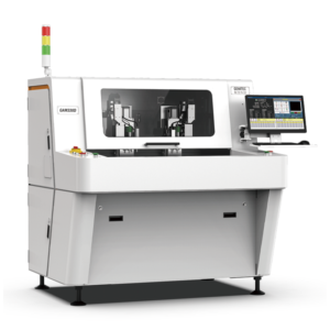

Stress levels exceeding 500μ strain during mechanical depaneling have been correlated with latent micro-cracking in Class 3 PCBs deployed in military avionics systems, where operational temperature cycling from -55°C to +125°C accelerates crack propagation at stress-concentrated edges. In Beijing-area research institutes and military contracting facilities, depaneling machines must maintain kerf tolerances of ±0.05mm to prevent ingress of conformal coating into routed slots and to ensure controlled impedance continuity across high-frequency RF circuits operating above 10GHz.
Stress Thresholds and Reliability Requirements in Military Applications
Military-grade PCB assemblies for radar systems, encrypted communications, and guidance electronics require depaneling processes that generate <350μ residual stress at the board edge, measured via strain gauge mapping per IPC-9701A guidelines. Depaneling machines equipped with 40,000-80,000 RPM air-cooled spindles and 0.8-2.0mm diameter carbide end mills must maintain chip load below 0.025mm per tooth to avoid delamination at the glass fiber/resin interface in high-Tg FR-4 (Tg≥170°C) and polyimide substrates. Feed rates are programmed at 0.5-2.0 m/min depending on panel thickness (0.8-3.2mm) and copper weight (1-4oz), with adaptive feed control engaging when spindle current draw exceeds 85% of rated capacity to prevent tool deflection that would violate the ±0.10mm profile tolerance required for AOI and ICT fixture registration.
Precision Depaneling for Research Institute Prototyping Workflows
Research institutes engaged in defense-related R&D operate under high-mix, low-volume production models where depaneling machines must accommodate panel sizes from 50×50mm test coupons to 400×500mm multi-up arrays within the same run. Tool changeover between 0.8mm and 2.0mm end mills must complete in <30 seconds to maintain throughput in prototyping workflows with 2-3 day design iteration cycles. Vision alignment systems with ±0.02mm repeatability compensate for panel distortion up to 0.15% occurring during reflow of large-format backplanes with 20+ layer counts. Depaneling programs must support Gerber input with real-time path optimization for irregular board shapes common in RF and microwave development, where edge-to-trace clearances as tight as 0.15mm require contour-following accuracy of ±0.03mm.
High-Speed Spindle Performance on Advanced Substrates
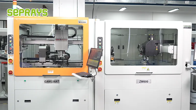
Spindle speed selection is governed by the critical chip thickness equation: at 60,000 RPM with a 1.0mm two-flute end mill, theoretical chip thickness at 1.0 m/min feed rate is 8.3μ, within the 5-15μ range required for clean cut quality in polyimide substrates used in space-grade flexible-rigid PCBs. Below 40,000 RPM, carbide tool wear accelerates due to increased cutting forces, with tool life dropping from 80-120 meters of cut length at optimum speed to <20 meters when speed falls below critical threshold. For halogen-free FR-4 formulations meeting outgassing requirements per NASA/ESA standards, feed rates must be reduced by 15-20% compared to standard FR-4 to accommodate the more brittle resin system, with cutting forces monitored via spindle motor current signature analysis.
Edge Quality and Contamination Control Requirements
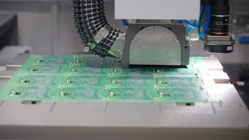
Research institutes manufacturing prototypes for radiation-hardened applications require depaneling in ISO Class 7 cleanroom environments where particle generation must be controlled to <100 particles/ft³ >0.5μ. Depaneling machines integrate HEPA-filtered chip extraction with 99.99% capture efficiency at 0.3μ, maintaining -15 to -25 Pa negative pressure to prevent fiberglass dust migration. Edge roughness (Ra) must be maintained below 3.2μ to prevent dendritic growth initiation sites in humid environments, measured via white light interferometry on batch samples. For boards with IAg or ENIG surface finishes, depaneling must complete within 4 hours of bake-and-reel to prevent edge-exposed copper from oxidizing beyond the 0.05μ oxide thickness limit compromising solder joint reliability in vibration-intensive military environments.
Process Validation and Standards Compliance
Depaneling process validation requires a Cpk report demonstrating Cpk≥1.33 across a minimum 30-piece run, with critical dimensions including board edge straightness (<0.10mm/100mm), corner radius consistency (±0.05mm), and minimum feature-to-edge distance (≥0.20mm for 0.15mm traces) documented per IPC-2221B Section 9. Depaneling machines must log spindle speed, feed rate, and tool position at 100ms intervals, with data retention for minimum 10 years supporting root-cause analysis of defense system field failures. For research institutes developing next-generation PCB technologies, depaneling compatibility testing must verify edge stress does not reduce fatigue life below 2,000 thermal cycles (0°C to 100°C, 15min dwell) per IPC-6012 Appendix A.
Technical Summary
PCB depaneling machines in Beijing-area research and military facilities must deliver ±0.05mm kerf tolerances, <350μ residual edge stress, and Cpk≥1.33 capability on substrates from standard FR-4 to polyimide and halogen-free formulations. Spindle speeds of 40,000-80,000 RPM with adaptive feed control and carbide tooling at <0.025mm per tooth chip load achieve the edge quality (Ra<3.2μ) and dimensional accuracy required for AOI, ICT, and functional test in high-reliability workflows. Compliance with IPC-2221B, IPC-6012 Class 3, and IPC-9701A is mandatory, with full process data logging and cleanroom-compatible extraction required for radiation-hardened and aerospace-grade PCB assemblies.
Recommended Equipment
Looking for proven depaneling solutions? Seprays offers a full range of equipment backed by 30+ years of industry experience. Here are two options worth considering for your production line:
- GAM330AT Fully Automatic PCB Depaneling Machine — Self-feeding operation with automatic sorting — ideal for high-volume automated production lines
- GAM310A Offline Automatic Board Separator — Compact single workbench with CCD visual correction — high precision in a small footprint
Frequently Asked Questions
Q1: What are the primary precision requirements for PCB depaneling in military and research institute applications compared to commercial production?
A1: Military and research institute applications typically demand positional accuracy of ±0.05mm or tighter, along with minimal mechanical stress during depaneling to protect sensitive components. Unlike commercial mass production where throughput is the primary metric, these environments prioritize cut edge quality and dimensional repeatability to meet stringent acceptance criteria such as IPC-A-610 workmanship standards. The consequence of tolerance stack-up in multi-board assemblies makes tight depaneling accuracy critical.
Q2: How do PCB depaneling machines adapted for classified or restricted-access environments handle security and traceability requirements?
A2: Specialized depaneling systems for defense and research applications often feature audit trail logging, operator authentication via RFID or PIN, and optional data export to MIL-STD-compliant formats for configuration management. Machine tool offsets, program revisions, and production timestamps are recorded to support as-built documentation requirements. Some configurations include isolated network interfaces to prevent unauthorized data egress while maintaining process control capability.
Q3: What spindle or cutting system specifications are most relevant for routing depaneling of specialized military PCB substrates such as high-frequency ceramics or heavy copper boards?
A3: For ceramic substrates or boards with copper weights exceeding 3oz, spindle speed typically ranges from 40,000 to 60,000 RPM with configurable down-cut and up-cut strategies to manage substrate cracking and burring. Spindle run-out must be controlled below 0.01mm to prevent delamination at the cut edge, particularly in RF/microwave boards where surface finish integrity is critical for electrical performance. Tool wear monitoring with automatic tool replacement or offset compensation becomes essential to maintain cut quality over extended production runs.
About Seprays
About Seprays Precision Machinery
Founded in 1993, Seprays has over 30 years of expertise in PCB depaneling solutions. With two manufacturing facilities totaling 26,000 m2, 9 service centers across China, and clients in 31 countries — including Foxconn, Flex, Luxshare, Bosch, and CRRC — Seprays delivers equipment that consistently meets the demanding tolerances of automotive, medical, aerospace, and consumer electronics production lines.
Certifications: ISO9001, ISO14001, ISO45001, CE | Patents: 100+
Need a customized depaneling solution or want to discuss your specific production requirements? Our technical team is ready to help.
Contact: jimmy@seprays.com