In the electronics manufacturing process, the depaneling (or splitting) of PCBA (Printed Circuit Board Assembly) is a critical step that significantly impacts product quality and reliability. The most common depaneling methods include stamp cutting, V-CUT, routing, and laser cutting. Each method has its own advantages, limitations, and suitable applications. Below is a detailed comparison:
1. Stamp Cutting
Advantages:
– High efficiency, suitable for high-volume production.
Disadvantages:
– High mechanical stress, which can easily cause circuit layer fractures;
– Poor precision control and low safety.
Typical Industries:
– Primarily used for low-end consumer electronics where precision requirements are low and cost is a key factor, such as simple toys and basic remote controls.
—
2. V-CUT Scoring
Advantages:
– High processing speed;
– Suitable for boards designed with V-grooves.
Disadvantages:
– Can easily damage the PCBA, leaving burrs along the cut edge;
– Poor dust control, risking contamination of components.
Typical Industries:
– Commonly used in household appliance control boards, standard LED lighting, power supply modules, and other industrial applications where high cleanliness and precision are not critical.
—
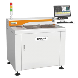
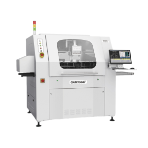
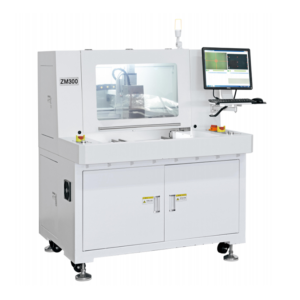
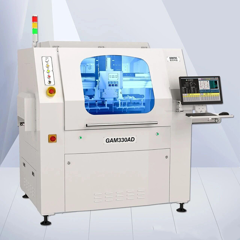
3. Routing (Milling)
Advantages:
– Burr-free cutting, low stress, and high precision;
– Effective dust extraction prevents contamination of components;
– Capable of cutting complex shapes; often includes vision compensation systems.
Disadvantages:
– Higher equipment cost compared to V-CUT or stamping.
Typical Industries:
– Widely used in telecommunications equipment, automotive electronics, medical electronics, industrial control systems, and other fields requiring high reliability.
—
4. Laser Depaneling
Advantages:
– Non-contact process, very low mechanical stress;
– Extremely high cutting accuracy.
Disadvantages:
– May cause carbonization or blackening on the cut surface;
– Lower cutting speed and higher equipment/maintenance costs.
Typical Industries:
– Ideal for flexible printed circuits (FPC), high-end microelectronic modules, wearable devices, aerospace electronics, and other applications with strict requirements for thermal impact and precision.
—
Summary & Recommendations
Stamp cutting and V-CUT methods impose high stress and offer limited precision and dust control, which can damage fragile solder joints and copper traces. Therefore, they are not recommended for high-reliability products.
To help select the right method for your industry, consider the following:
– Consumer Electronics & Home Appliances: V-CUT or stamp cutting (if cost is a major constraint).
– Automotive, Telecom, & Industrial Control: Routing is strongly recommended.
– High-End Microelectronics, Flex Circuits, Medical Devices: Laser depaneling is the preferred choice.
If you have specific product requirements or process questions, feel free to reach out for customized depaneling solutions.