Printed Circuit Boards (PCBs) are fundamental components in nearly all electronic devices, ranging from consumer electronics to industrial equipment. The manufacturing process involves multiple precise stages to ensure reliability, functionality, and performance. This guide outlines the key steps in PCB production, with a focus on depaneling, and introduces the role of advanced automation in enhancing efficiency and quality.
1. Material Cutting (Panelization)
Standard PCB panel sizes—such as 939×1245mm, 1092×1245mm, and 2041×1245mm—are utilized to maximize material efficiency. The full copper-clad laminate is cut into smaller work panels for streamlined processing.
2. Surface Grinding
The copper surface undergoes grinding and polishing to eliminate oxides, contaminants, and surface roughness. This step improves adhesion for subsequent chemical and imaging processes.
3. Inner Layer Circuitry
This stage includes dry film lamination, exposure, development, etching, strip-off, and Automated Optical Inspection (AOI). Circuit patterns are accurately formed on the inner layers through photolithography.
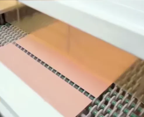
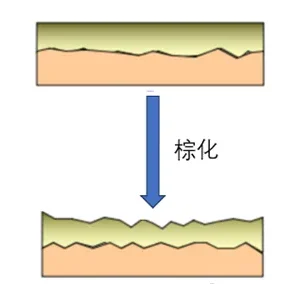
4. Browning (Oxide Treatment)
A brown oxide layer is chemically grown on the copper surface. This enhances bond strength between the core material and prepreg (PP), reducing risks of delamination or blowholes during lamination.
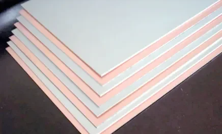
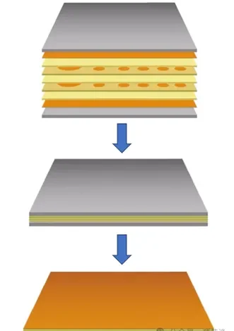
5. Lamination
Multiple circuit layers are bonded using prepreg and a vacuum hot press. This process forms a solid multilayer PCB structure under controlled temperature and pressure.
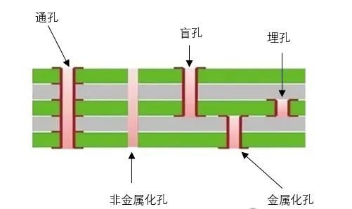
6. Drilling
Drilling machines create through-holes, blind vias, and buried vias for electrical interconnection and component mounting. Both plated and non-plated holes are produced as per design.
7. Hole Inspection
Drilled holes are verified for dimensional accuracy and positional tolerance against design data to ensure reliability before further processing.
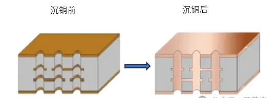
8. Electroless Copper Deposition
A thin conductive copper layer is chemically deposited on non-conductive hole walls, providing a base for subsequent electroplating.
9. Electroplating
Electroplating increases copper thickness on surface traces and inside holes, improving conductivity, mechanical strength, and reliability.
10. Microsection Testing
Cross-section samples are prepared, polished, and analyzed under a microscope or SEM to verify plating quality, layer alignment, and internal integrity.
11. Outer Layer Circuitry
Similar to inner layers, outer circuit formation uses either positive or negative film processes. Additional copper plating and tin-lead etching resist may be applied for fine-line patterning.
12. Solder Mask Application
A solder mask ink (commonly green, but also available in blue, black, red, etc.) is applied to protect copper traces and prevent solder shorts.
13. Silkscreen Printing
Component designators, logos, and other identifiers are printed onto the board surface using epoxy ink.
14. Surface Finish
Exposed copper areas receive a protective coating such as ENIG (Electroless Nickel Immersion Gold), Immersion Silver, OSP (Organic Solderability Preservative), or Immersion Tin to ensure solderability and prevent oxidation.
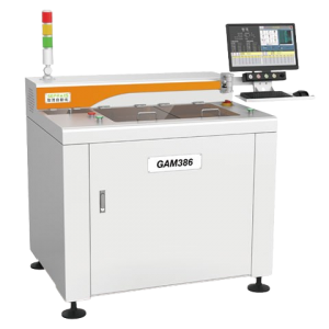
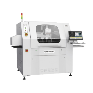
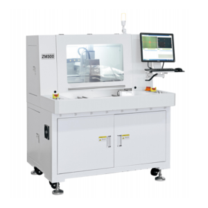
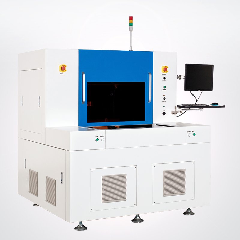
15. Routing and Depaneling
The assembled panel is cut into individual PCBs using a PCB router machine or PCB depaneling machine. V-cut scoring or tab routing is applied for smooth, stress-free separation.
16. Electrical Testing, Cleaning, and Packaging
Each board undergoes electrical testing (e.g., flying probe), cleaning to remove residues, final quality control (FQC), and packaging for shipment.
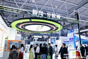
Seprays: Advancing PCB Automation
Seprays specializes in high-precision PCB automation solutions, including advanced PCB depaneling machines. Their equipment ensures accurate, efficient, and low-stress separation of circuit boards, supporting high-volume and high-mix production. With a focus on innovation and reliability, Seprays helps manufacturers improve yield, reduce labor costs, and maintain consistent quality in PCB fabrication and assembly.